MSP430 Tutorial
Posted: January 14, 2023
Introduction
Here's some "getting started" guide on programming MSP430 chips using naken_asm as an assembler and mspdebug to flash the chips and debug them. This tutorial will hopefully be useful for someone who:
- Comes from the software world and wants to know how microcontrollers work.
- Want to learn about the different features of MSP430's that can be used.
- Learn some simple MSP430 assembly.
- Learn how to program these chips without a big IDE to download.
Concepts that will be discussed on this page:
- Microcontrollers
- MSP430 CPU
- Assembling and Running Code
- Debugging Code
- Clock Sources
- Peripherals
- Digital I/O
- Timers
- Analog to Digital converters (ADC)
- UART
- SPI
- i2c
- Using Transistors
If something needs more explanation or such, feel free to send me an email so I can add to this page. I've been tempted to do a video for this too, but not sure if that's useful.
I also started an MSP430 code builder to possibly help assist writing programs.
Microcontrollers
A microcontroller is basically a microchip that contains a CPU, RAM, flash memory (to hold the firmware / computer program), peripherals (digital I/O, timers, analog/digital converters, SPI, i2c), and more all embedded in a single chip. Most chips run between 1MHz to 20MHz in speed and have 8, 16, or 32 bit instruction sets.
Most of the projects on this website use either Atmel AVR8 (ATtiny85, ATtiny2313) or MSP430 (MSP430G2553, MSP430G2231). So how do I pick which chip to use? Each of these chips have different features and different limitations. The MSP430 have the Launchpad for a really easy debugger (as will be shown later) while the Atmel chips are really not that easy, especially on Linux. Atmel chips have an advantage that they can run at +5v or 3.3v while MSP430 is 1.8v to 3.3v. Which means interfacing with 5v devices is much much simpler with the Atmel chips. The ATtiny85 is only 8 pins (four on each side) making it really nice for very small circuits. The Atmel AVR8 chips have an 8 bit instruction set while the MSP430 is a 16 bit instruction set.
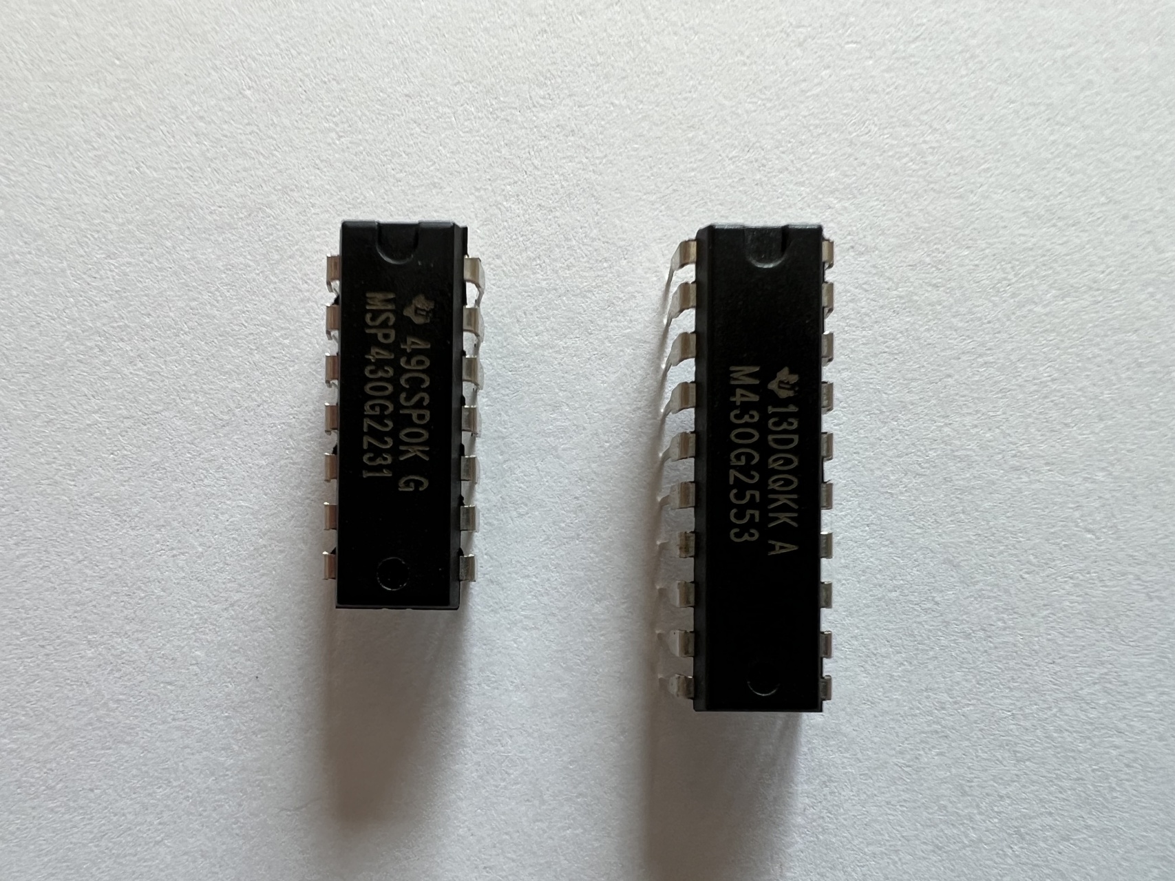
Above is both an MSP430G2231 and MSP430G2553. The first obvious difference is the MSP430G2231 has only 16 pins while the MSP430G2553 has 20. If not that many pins are needed for the circuit, it's probably better to pick the smaller chip. However, the MSP430G2553 not only has more pins, but it also has things like a hardware UART. The functions of the pins are almost identical so there's a possibility that if the circuit has an MSP430G2553 in it, the chip can be drop in replaced with the smaller MSP430G2231. Just be careful with SPI, the data pins are swapped between the two chips. Another important difference between the chips is the MSP430G2553 has 16 kB flash / 512 bytes RAM while the MSP430G2231 has 2kB flash / 128 bytes RAM.
The chips themselves come in different packages, where the package is the casing that the chip is covered by. When ordering raw chips from a site like Mouser, make sure to look for PDIP16 or PDIP20 packages like the ones in the picture above. These packages are through-hole and can be easily placed in a breadboard. They sell these chips in surface mount packages which have smaller pins and must be soldered on top of a board created for that packaging.
MSP430 Core
Wikipedia has a list of MSP430 instructions along with their opcode bit encodings. A quick list of the instructions are:
Instruction Description rrc <dst> Rotate right through carry. rra <dst> Rotate right arithmetic. swpb <dst> Swap upper / lower bytes. sxt <dst> Sign extend 8 bit value to 16 bit. push <dst> Push value to stack. call <dst> Call a function. reti Return from interrupt. mov <src>, <dst> Copy value from src to dst. add <src>, <dst> dst = dst + src. addc <src>, <dst> dst = dst + src + c. subc <src>, <dst> dst = dst - src. sub <src>, <dst> dst = dst - src + c. cmp <src>, <dst> dst - src (don't store result, but set flags) dadd <src>, <dst> dst = dst + src (BCD mode). bit <src>, <dst> dst & src (don't store result, but set flags) bic <src>, <dst> dst = dst & ~src (clear bits) bis <src>, <dst> dst = dst | src (set bits) xor <src>, <dst> dst = dst ^ src and <src>, <dst> dst = dst & src jne / jnz <address> Jump if not equal / zero. jeq / jz <address> Jump if equal / zero. jnc / jlo <address> Jump if no carry / lower (unsigned). jc / jhs <address> Jump if carry / higher or same (unsigned). jn <address> Jump if negative flag set. jge <address> Jump if greater than or equal (signed). jl <address> Jump if less (signed). jmp <address> Jump always.
MSP430 assemblers also understand "pseudo-operations" which don't really exist in the instruction set above, but will output an equivalent instruction:
Alias Actual Instruction Description clrc bic.b #1, SR Clear carry flag. clrn bic.b #4, SR Clear negative flag. clrz bic.b #2, SR Clear zero flag. setc bis.b #1, SR Set carry flag. setn bis.b #4, SR Set negative flag. setz bis.b #2, SR Set zero flag. dint bic.b #8, SR Disable interrupts. eint bis.b #8, SR Enable interrupts. nop mov.w #0, r3 No operation. ret mov @SP+, PC Return from function (opposite of call). pop <dst> mov @SP+, <dst> Pop from stack (opposite of push). clr.x <dst> mov.w #0, <dst> Clear destination. adc.x <dst> addc.w #<dst> Add carry to destination. br <dst> mov <dst>, PC Branch to destination. dadc.x <dst> dadd.w #0, <dst> Decimal add carry destination. dec.x <dst> sub.w #1, <dst> Decrement. decd.x <dst> sub.w #2, <dst> Decrement by 2. inc.x <dst> add.w #1, <dst> Increment. incd.x <dst> add.w #2, <dst> Increment by 2. inv.x <dst> xor.x #-1, <dst> Invert. rla.x <dst> add.w <dst>, <dst> Rotate left arithmetic. rlc.x <dst> addc.w <dst>, <dst> Rotate left through carry. sbc.x <dst> subc.w #0, <dst> Subtract borrow from destination. tst.x <dst> cmp.w #0, <dst> Test if destination is 0.
These are instructions that despite having a name like "inc" is really just an alias for "add". So assembling:
inc.w r8
Will actually output the instruction:
add.w #1, r8
The MSP430 has 16 registers labeled PC (program counter), SP (stack pointer), SR (status register), CG (constant generator), and r4 through r15. Registers r4 to r15 are fair game, but the first four registers are rarely accessed directly. The CG register is never accessed by the developer, it's used by the assembler so that when using 1, 2, 4, 8, or -1 are used as an immediate value, the instruction can be encoded as 16 bits. For example:
  mov.w #1, r8

0x0006: 0x4318 mov.w #1, r8                             cycles: 1
  mov.w #3, r8

0x0006: 0x4038 mov.w #0x0003, r8                        cycles: 2
0x0008: 0x0003
In the two examples above, the first sets register r8 to the number 1. This can be done as a single 16 bit encoding and only takes 1 CPU cycle to execute. The assembler actually encoded the source register as "CG" and the 2 bit source addressing mode flags to 01 telling the CPU to load a constant of 1 into the r8. In the second example, #3 cannot be generated by the CG register, so the immedate value is the next 16 bits after the instruction causing it to use 32 bits and take 2 cycles to execute.
Most instructions can take a .b or .w flag that let the assembler know if operation should be 8 bit or 16 bit (word). 16 bit accesss to memory are done little endian (least significant byte first). So if the program writes 0x1234 as 16 bit to location 0x200 in memory, the memory address 0x200 will contain 0x34 and address 0x201 will contain 0x12. There are several addressing modes for every instruction, all can be used in the source operand but only 2 of them can be used for the destination.
mov.w r8, r9 (copy register r8 to r9)
mov.w @r8, r9 (copy 16 bits from address r8 points to to r9) mov.w @r8+, r9 (copy 16 bits from address r8 points to to r9
r8 = r8 + 2) mov.b @r8+, r9
(copy 8 bits from address r8 points to r9
r8 = r8 + 1) mov.w 0x80(r8), r9
(copy 16 bits from address r8 points to plus 80
to r9. So if r8 = 0x200, copy address 0x200
and 0x201 as little endian) mov.w &0x200, r9
(copy 16 bits from 0x200 / 0x201 little endian
into r9) mov.b &0x200, r9 (copy 8 bits from 0x200 to r9) mov.b 0x200, r9 (copy 8 bits from 0x200 to r9) mov.w r8, &0x200
(copy 16 bits from r8 to memory address
0x200 / 0x201 little endian) mov.w r8, 0x80(r9)
(copy 16 bits from r8 to memory address
r9 + 0x80 (and r9 + 0x81) little endian) mov.w #5, r9 (copy 5 to r9) mov.b #5, r9 (copy 5 to r9)
Note in the mov.w #5, r9 and mov.b #5, r9 instructions are basically identical since they will both instructions take up 32 bits as opcodes. All instructions will be a multiple of 16 bits, so even though moving a byte with a value of 5 is only 8 bits, the 16 bit little endian value of 0x05 0x00 will still be written to program memory. Also, if it's not obvious the syntax of the chip is <instruction> <source>, <destination>.
Any instruction that treats a register as 8 bits will clear the upper 8 bits of the register.
mov.w #0x1234, r8
add.b #1, r8
After those two instructions run, r8 will hold the value 0x0035.
Another thing to notice is when using an address as either a source or destination, it can be done with an & infront or without (in the above &0x200 vs 0x200). The difference is & uses the address as an absolute address. If the code is disassembled, 0x200 with be in 16 bits after the opcode. Without the & it it's assembled using an offset from the current instruction to the address. The purpose is using & or without is to make the code relocatable. Any reference to a hardware register should have & while reference to data in flash memory could be done without so if the code is memcpy()'d to a different address, it will still execute the same.
Hooking Up The Chips
Each of these chips has a black casing and a number of pins coming out of the bottom. Each one of those pins has a specific function and to figure out what they do, the manufacturer of the chip will show a pinout map in their datasheets. Since links can move, there won't be any links to the Texas Instruments PDF's for the MSP430, but doing a web search for "msp430g2553 datasheet" will bring up a page that has both the MSP430G2553 datasheet and the MSP430G2xx Family User Guide. Both are needed. The MSP430G2xx Family User Guide is for all chips that start with the number 2 (including the MSP430G2231) while the MSP430G2553 PDF will have the information specific for this chip. Below is both the chip and the pinout:
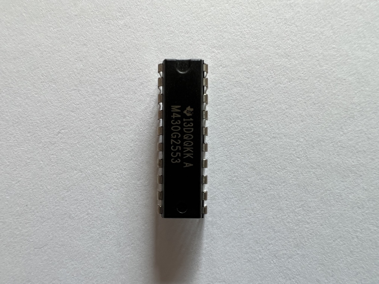
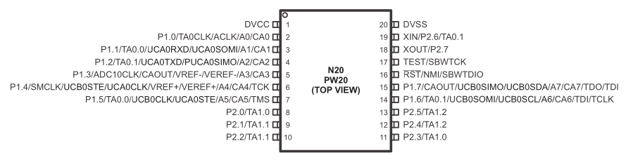
The first thing to notice is all the pins are numbered from 1 to 20. The top left pin is always pin 1 and the top right pin is always the highest number pin. The very top of the chip has a notch carved out on it. This is how to tell where the top of the chip is. On some chips they will instead carve out a circle next to pin 1, but this one has the notch.
Another thing to notice, most of those pins have multiple labels separated by a slash. For example, pin 2 has P1.0 / TA0CLK / ACLK / A0 / CA0. This pin can be configured to do multiple things (not at the same time of course) by placing a value in a configuration register. By default on this chip, the pins are configured to be P1.0 to P1.7. Pins 8 to 13 default to P2.0 to P2.5. Table 2 in the MSP430G2553 PDF will explain what all these functions are. More on this later.
There is a minimum of 3 pins that are used to "turn on" the chip. DVcc must be connected to a positive voltage source, 1.8 is minimum and 3.3v is maxiumum. Hooking this chip up to more than 3.6v will cause it to get warm and can cause it to do weird stuff including damaging it. DVss needs to be connected to GND of the power source (the negative terminal of a battery). The D in DVcc / DVss means digital. Some chips do this because they might have an AVcc power connection for analog circuitry. Also, some chips will label Vcc as Vdd and Vss as just GND. In order for this chip to run, the /RST chip should be connected with a 47k ohm resistor to DVcc. Why 47k ohms? Because the datasheet says so. The MSP430G2 Launchpad schematic also shows 47k ohms with a 1000pF capacitor to GND. I usually leave off the capacitor.
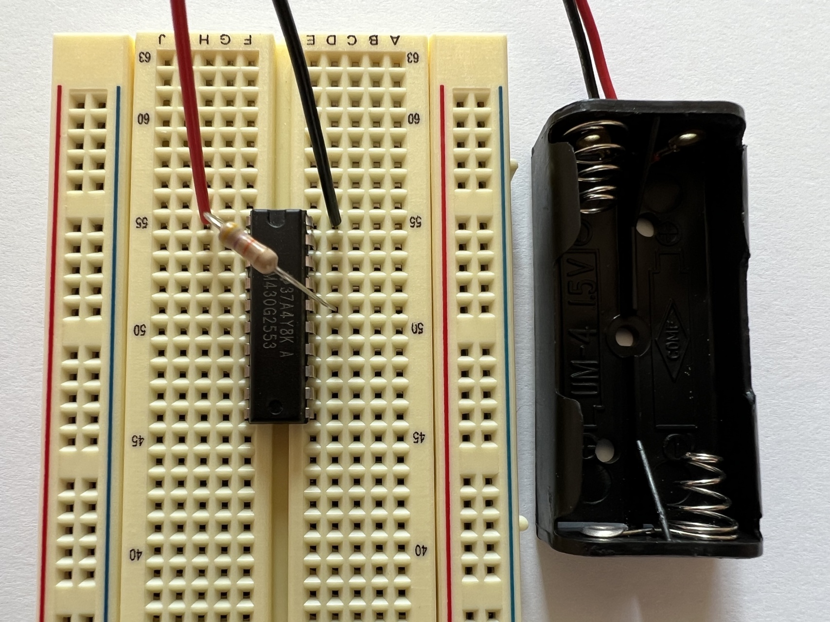
Above shows an MSP430 in a breadboard. The resistor is connected from /RST to DVcc. The battery clip holds 2 AAA batteries which are 1.5v each or 3.0v total when hooked up in series. The +3v wire is connected to pin 1 on the microcontroller while GND is connected to pin 20. If there was a program on this chip and there were batteries in that pack it would start executing. As a tip, figure out a good color coding for wires and stick with it to make circuits easier to read. For example red = +v, black = gnd, blue = data, white = chip select, yellow = clock, etc.
The next step here would be to hook up something interesting to the chip and the MSP430G2 Launchpad as a debugger.
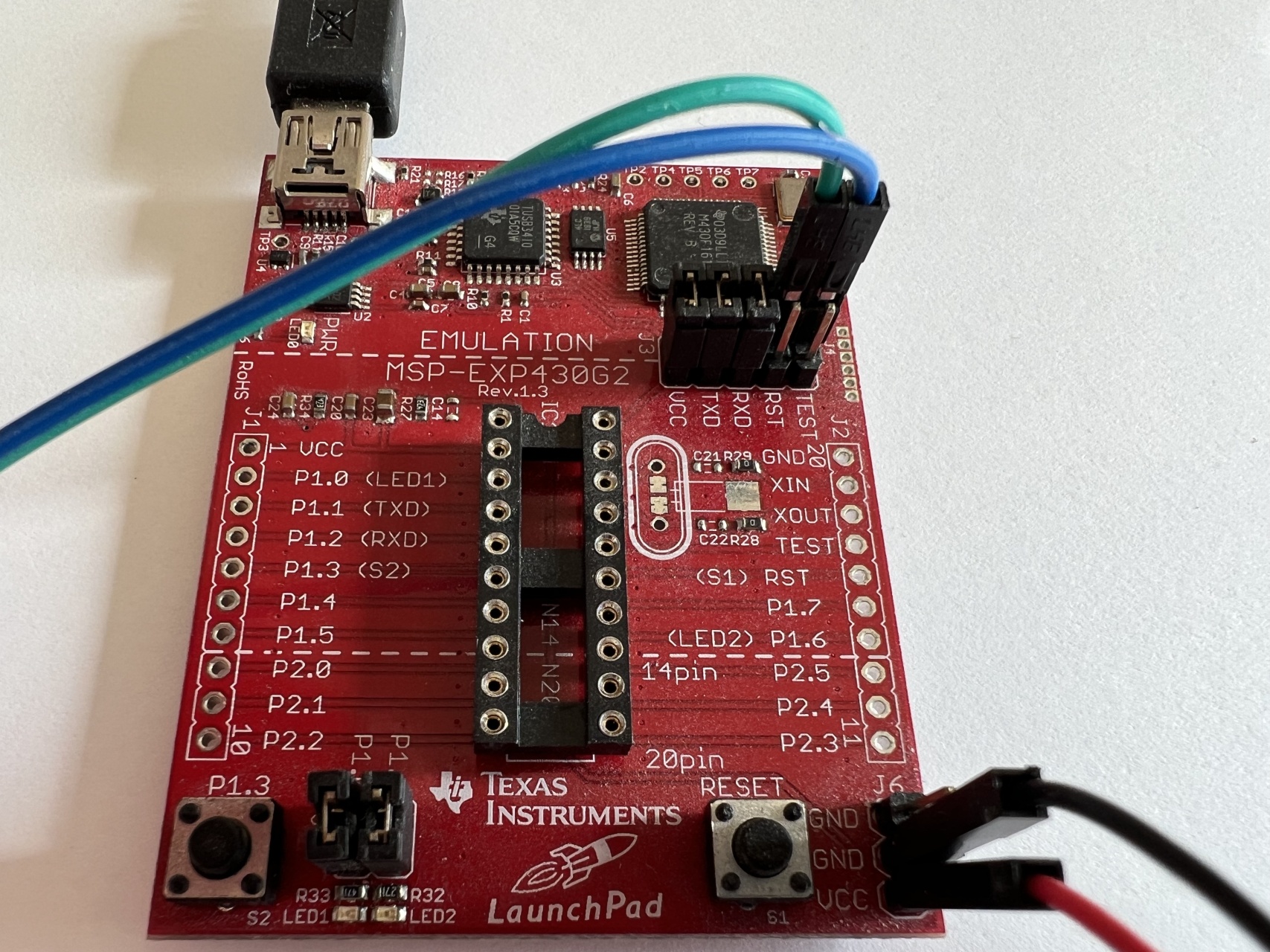
The picture above shows the MSP430G2 Launchpad with the chip removed from the socket. At the bottom right is a black jumper connected to GND and a red wires connected to Vcc. Those two wires will be connected to DVcc and DVss on the breadboard. At the upper right there are a set of jumpers with their function silk screened on the board. The RST and TEST jumpers have been removed and a blue wire is connected to the far side of TEST and a green jumper connected to RST. Those two pins wires will be connected to RST and TEST pins on the MSP430G2553. These allow the Launchpad to act like a debugger to the chip using a Spy-By-Wire protocol. Note that if the MSP430G2553 is powered separately, do not connect the red wire to Vcc, but the GND wire must be connected to the circuit.
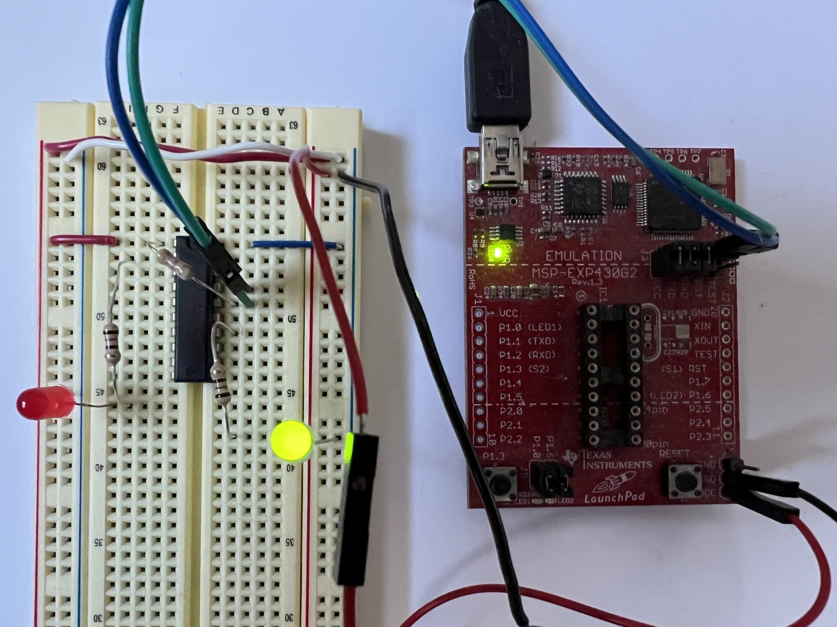
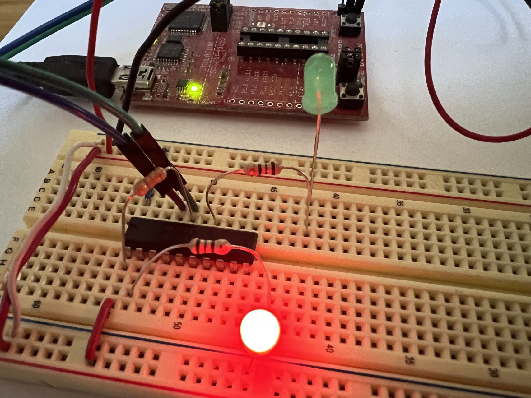
Above is the breadboard being powered by the launchpad. At the top of the bread board connects the red / blue rails on either side so that both sides of the breadboard have +3.3v and GND connections. DVcc and DVss are connected to power and TEST / RST are connected to the blue / green wires to the launchpad. P1.0 and P1.6 are connected to a 180 ohm resistor to an LED to ground.
Above is another view of the circuit.
The pins when configured as digital I/O (on some chips called general purpose I/O or GPIO) are labeled P1.0 to P1.7. These are pins 2 to 7 for P1.0 to P1.5 and pins 14 and 15 for P1.6 to P1.7. As digital I/O they can be inputs or outputs. If configured as outputs they will have a voltage on them or 0 volts. The voltage they will output is the same voltage as DVcc, so if the chip is running at 3.3v, then they will output 3.3v when set to 1. When set to 0 they can actually sink voltage, so if there is an LED hooked up to them backwards (from 3.3v through the LED in the correct direction to GND) they will turn on when the output is 0 and turn off when the output is 3.3v.
A few things to note about the LED part of the circuit. The first is LED only work in one direction. If you put +3.3v on the short pin and GND on the long pin, they won't turn on. But if you put 3.3v on the long pin and 0v on the short they will. The next thing to note is an LED needs to limit the amount of current. These cheap LEDs on the circuit above can't have more than 20mA of current through them. The last thing to note is there is a limit on the amount of current you can pull from a microcontroller without the possibility of either glitches in the code or damage to the pin. Most microcontrollers limit to 20mA, I believe in this chips case you can't pull more than 20mA on all the pins combined.
To limit the amount of current pulled from the microcontroller a
resistor is used. The formula is ohms' law current = voltage / resistance.
Sending a voltage through a diode causes a voltage drop too, in this
case it's around 1.7v for this LED, so the forumula is:
(3.3v - 1.7v) / 180 ohm = 0.0088A or ~9mA
If the device (LED, motor, etc) needs more current to operate, a transistor can be used. A transistor can act like a switch so when there is a small current at the base pin, a large current (or voltage) can pass through the transistor and into the LED or motor. It's probably a good idea to use transistors on a circuit with many LEDs even if only 1 or 2 are needed to be on at one time incase there is a bug in the circuit and they all accidentally turn on. More on transistors later.
To turn pins P1.0 and P1.6 on and off using code the first thing that needs to be done is to configure them as outputs and then give them a value:
  mov.b #0x41, &P1DIR
  mov.b #0x40, &P1OUT
P1DIR and P1OUT are defined in include/msp430/msp430x2xx.inc. They are hardware registers (not to be confused with CPU registers) that can be written to and read from like RAM, but changing their value will change the behavior of the MSP430's input / output pins. The hardware registers are used to configure the peripherals on the chip. The trick for digital I/O is to imagine the array of pins P1.7 to P1.0 as a binary number. In the above example:
       P1.7 P1.6 P1.5 P1.4 P1.3 P1.2 P1.1 P1.0
P1DIR    0    1    0    0    0    0    0    1   = 0x41
P1OUT    0    1    0    0    0    0    0    0   = 0x40
So P1.6 and P1.0 in the P1DIR register have a value of 1 so they are configured as outputs. P1.6 is 1 and P1.0 is 0 so P1.6 (pin 14) is going to output 3.3v and P1.0 (pin 2) will output 0v. Because there are LEDs on those pins, when they are outputting 3.3v the LEDs turn on. Since the rest of the pins are configured as input, if the P1.1 pin (pin 3 on the MSP430G2553) is connected to 3.3v through a resistor (use 20k to 50k) a register P1IN will have a value:
       P1.7 P1.6 P1.5 P1.4 P1.3 P1.2 P1.1 P1.0
P1IN     0    0    0    0    0    0    1    0   = 0x02
The value can be easily read with code like:
mov.b &P1IN, r8
Note that these digital I/O registers must be read / written to with 8 bit instructions.
Downloading Software
On Ubuntu mspdebug can be installed by using:
sudo apt install mspdebug
There are precompiled binaries for Windows and Mac for naken_asm and a tarball with source code, but really the best thing is to clone the repo. That can be done by executing the following commands from the terminal:
sudo apt install libreadline-dev   (not required, but nice to have)
git clone https://github.com/mikeakohn/naken_asm.git
cd naken_asm
./configure
make
This will create binaries for naken_asm (the assembler) and naken_util which is a utility that can disassemble code and also contains a simulator for some CPUs, including the MSP430. This means an MSP430 program can be assembled with naken_asm and executed step by step in software with the ability to examine registers and memory and such.
The naken_asm repo also contains documentation and sample code.
Assembling and Running launchpad_blink.asm
In the samples directory of naken_asm is small program called launchpad_blink.asm. This program will blink the two LEDs in the circuit above, but would also blink the two LEDs on the Launchpad itself since they are connected to P1.0 and P1.6 also. To assemble it the following can be done:
mike@falkenberg:/code/git/naken_asm/samples/msp430$ ../../naken_asm \
  -l -I../../include/msp430 -o launchpad_blink.hex launchpad_blink.asm

naken_asm

Authors: Michael Kohn
         Joe Davisson
    Web: http://www.mikekohn.net/
  Email: mike@mikekohn.net
Version: January 8, 2023

 Input file: launchpad_blink.asm
Output file: launchpad_blink.hex
  List file: launchpad_blink.lst

Pass 1...
Pass 2...

Program Info:
Include Paths: .
               ../../include/msp430
               /usr/local/share/naken_asm/include
               include
 Instructions: 9
   Code Bytes: 32
   Data Bytes: 2
  Low Address: f800 (63488)
 High Address: ffff (65535)
There are some extra command line arguemnts there. The -o tells the assembler that the output filename should be called launchpad_blink.hex. Normally it would default to out.hex. The -l tells the assembler to generate a launchpad_blink.lst file which contains all of the source code from launchpad_blink.asm along with the opcode that got generated for each instruction plus how many CPU cycles that instruction would take to execute. The -I option tells what directory to look in to find any .include files.
To copy the .hex file from the computer to the MSP430 is done with mspdebug like so:
mike@falkenberg:/code/git/naken_asm/samples/msp430$ mspdebug rf2500
MSPDebug version 0.22 - debugging tool for MSP430 MCUs
Copyright (C) 2009-2013 Daniel Beer <dlbeer@gmail.com>
This is free software; see the source for copying conditions.  There is NO
warranty; not even for MERCHANTABILITY or FITNESS FOR A PARTICULAR PURPOSE.

Trying to open interface 1 on 009
rf2500: warning: can't detach kernel driver: No data available
Initializing FET...
FET protocol version is 30066536
Set Vcc: 3000 mV
Configured for Spy-Bi-Wire
fet: FET returned error code 4 (Could not find device or device not supported)
fet: command C_IDENT1 failed
Using Olimex identification procedure
Device ID: 0x2553
  Code start address: 0xc000
  Code size         : 16384 byte = 16 kb
  RAM  start address: 0x200
  RAM  end   address: 0x3ff
  RAM  size         : 512 byte = 0 kb
Device: MSP430G2xx3
Number of breakpoints: 2
fet: FET returned NAK
warning: device does not support power profiling
Chip ID data: 25 53

Available commands:
    =           erase       isearch     power       save_raw    simio
    alias       exit        load        prog        set         step
    break       fill        load_raw    read        setbreak    sym
    cgraph      gdb         md          regs        setwatch    verify
    delbreak    help        mw          reset       setwatch_r  verify_raw
    dis         hexout      opt         run         setwatch_w

Available options:
    color                       gdb_loop
    enable_bsl_access           gdbc_xfer_size
    enable_locked_flash_access  iradix
    fet_block_size              quiet
    gdb_default_port

Type "help <topic>" for more information.
Use the "opt" command ("help opt") to set options.
Press Ctrl+D to quit.

(mspdebug) prog launchpad_blink.hex
Erasing...
Programming...
Writing   32 bytes at f800...
Writing    2 bytes at fffe...
Done, 34 bytes total
(mspdebug) run
Running. Press Ctrl+C to interrupt...
^C
    ( PC: 0f81a)  ( R4: 03bfd)  ( R8: 00040)  (R12: 00000)
    ( SP: 003fe)  ( R5: 0edfc)  ( R9: 05e50)  (R13: 0ffe9)
    ( SR: 00001)  ( R6: 07f57)  (R10: 07fda)  (R14: 0fffe)
    ( R3: 00000)  ( R7: 0ebdd)  (R11: 0dedf)  (R15: 072e1)
0xf81a:
    0f81a: 19 83                     DEC     R9
    0f81c: fe 23                     JNZ     0xf81a
    0f81e: f7 3f                     JMP     0xf80e
    0f820: ff ff ff ff               AND.B   @R15+,  0xffff(R15)
    0f824: ff ff ff ff               AND.B   @R15+,  0xffff(R15)
    0f828: ff ff
(mspdebug)
The above shows using the "prog" command to copy the program from the computer to the MSP430. The "run" command tells the MSP430 to start executing the code. Pressing ctrl-C will stop the program and dump the registers along with a disassembly of the currently executing instruction.
If the running program had code like this:
  mov.b #0x20, r8
  mov.w #0x1234, r9
  mov.b r8, &0x200
  mov.b #0x21, &0x201
  mov.w r9, &0x202
Some memory would be set in the MSP430:
(mspdebug) md 0x200
    00200: 20 21 34 12 90 0d 04 c6 00 12 1a 26 52 b0 6c 6a | !4........&R.lj|
    00210: 22 40 60 80 66 66 82 48 08 0a 28 28 03 40 01 12 |"@`.ff.H..((.@..|
    00220: 00 d9 21 4a 20 26 02 02 12 08 08 40 00 40 01 06 |..!J &.....@.@..|
    00230: f2 34 10 90 88 2c 95 80 c2 92 90 2e 49 80 02 08 |.4...,......I...|
(mspdebug)
In mspdebug the "md" command can be used to examine memory.
Launchpad Blink
The launchpad_blink.asm looks like this:
.msp430
.include "msp430x2xx.inc"

.org 0xf800
start:
  ;; Turn off watchdog timer.
  mov.w #WDTPW|WDTHOLD, &WDTCTL

  ;; Set P1.0 and P1.6 as outputs.
  mov.b #0x41, &P1DIR

main:
  ;; Initial value for LEDs turns on the P1.0 LED and
  ;; keeps P1.6 turned off.
  mov.w #0x01, r8
while_1:
  ;; Set LEDs to current value of r8 and toggle P1.0 and P1.6.
  mov.b r8, &P1OUT
  xor.b #0x41, r8

  ;; Delay by decrementing r9 60000 times.
  mov.w #60000, r9
delay_loop:
  dec r9
  jnz delay_loop

  ;; Repeat loop.
  jmp while_1

.org 0xfffe
  dw start             ; set reset vector to 'init' label
The first thing this program done is disables the watchdog timer. A watchdog timer is a counter that starts at 0xffff and decrements by 1 every clock cycle. If it ever reaches 0, the system will reset. So if the watchdog timer is running, the software will need to periodically set the timer back to 0xffff to make sure it doesn't reset. This can be useful if the system needs a fail-safe to recover from a crash. If the chip hangs and doesn't "kick the dog" the system can reset and hopefully recover. In this case (and in most cases) it's just annoying so it's turned off. Most systems don't enable the watchdog by default, but MSP430 seems to.
To create a delay loop between toggling the LEDs, a simple loop is created. The r9 register starts at a value of 60000 and decrements until it reaches 0. It takes 1 cycle to do the dec.w r9 and 2 cycles to jnz (jump if not zero) back to the dec.w instructions. So that delay will be 60,000 * 3 = 180,000 cycles. If the chip is running at 1MHz then it will blink 1,000,000 / 180,000 = 5.5 times a second.
Clock Sources
The clock source will define how many CPU cycles per second the chip will get for executing instructions (or running timers). The MSP430 can have multiple clock sources and run different peripherals with those different clock sources. For example a 32.768kHz crystal can be attached to the XIN/XOUT pins and one of the timers can be configured to use it, while another timer is configured to use the main system clock.
For these cheaper MSP430 chips, the system clock is probably going to be something called the DCO. The DCO is done with an internal resistor and capacitor I believe. It can be configured to run below 1MHz all the way up to above 16MHz, which will cause the chip to glitch all over the place. The DCO is also very inaccurate. Its heavily affected by temperature. It's really best not to run the chip above 8MHz and for most things 1MHz works great. Also, the slower the speed, the longer the battery will last if it runs on battery.
In order to set the DCO speed, there are two constants to use: DCO_x (DCO speed) and RSEL_x (range select):
  ;; Set MCLK to 16 MHz with DCO
  mov.b #DCO_4, &DCOCTL
  mov.b #RSEL_15, &BCSCTL1
  mov.b #0, &BCSCTL2
To test the actual clock speed of the DCO on two different MSP430G2553 chips, I used a circuit that had a 32.768kHz crystal (a very very accurate clock source) setup with one the MSP430G2553's timers so it would trigger an interrupt once a second and count how many DCO cycles passed over that time. I ended up with these results:
DCO_0 DCO_1 DCO_2 DCO_3 DCO_4 DCO_5 DCO_6 DCO_7
RSEL_0 - 0.096MHz 0.102MHz 0.110MHz 0.119MHz 0.130MHz 0.142MHz 0.157MHz
RSEL_1 0.112MHz 0.119MHz 0.127MHz 0.137MHz 0.148MHz 0.161MHz 0.177MHz 0.196MHz
RSEL_2 0.155MHz 0.165MHz 0.176MHz 0.189MHz 0.205MHz 0.223MHz 0.245MHz 0.271MHz
RSEL_3 0.219MHz 0.233MHz 0.249MHz 0.268MHz 0.290MHz 0.315MHz 0.346MHz 0.383MHz
RSEL_4 0.300MHz 0.319MHz 0.342MHz 0.367MHz 0.396MHz 0.432MHz 0.473MHz 0.524MHz
RSEL_5 0.428MHz 0.456MHz 0.487MHz 0.523MHz 0.566MHz 0.615MHz 0.674MHz 0.745MHz
RSEL_6 0.588MHz 0.626MHz 0.669MHz 0.718MHz 0.775MHz 0.843MHz 0.924MHz 1.021MHz
RSEL_7 0.834MHz 0.886MHz 0.946MHz 1.016MHz 1.096MHz 1.190MHz 1.303MHz 1.440MHz
RSEL_8 1.181MHz 1.255MHz 1.339MHz 1.436MHz 1.549MHz 1.680MHz 1.838MHz 2.031MHz
RSEL_9 1.710MHz 1.815MHz 1.935MHz 2.074MHz 2.233MHz 2.421MHz 2.646MHz 2.919MHz
RSEL_10 2.459MHz 2.607MHz 2.776MHz 2.971MHz 3.195MHz 3.459MHz 3.779MHz 4.165MHz
RSEL_11 3.061MHz 3.250MHz 3.464MHz 3.714MHz 4.004MHz 4.338MHz 4.742MHz 5.256MHz
RSEL_12 4.191MHz 4.441MHz 4.727MHz 5.066MHz 5.468MHz 5.930MHz 6.460MHz 7.100MHz
RSEL_13 5.833MHz 6.169MHz 6.538MHz 6.963MHz 7.478MHz 8.118MHz 8.911MHz 9.891MHz
RSEL_14 8.422MHz 8.944MHz 9.543MHz 10.217MHz 11.008MHz 11.895MHz 12.920MHz 14.140MHz
RSEL_15 11.744MHz 12.369MHz 13.048MHz 13.813MHz 14.754MHz 15.981MHz 17.551MHz 19.405MHz
Running the exact same firmware on another MSP430G2553 chip got these quite different results:
DCO_0 DCO_1 DCO_2 DCO_3 DCO_4 DCO_5 DCO_6 DCO_7
RSEL_0 - - - - - 0.126MHz 0.139MHz 0.154MHz
RSEL_1 - - 0.124MHz 0.133MHz 0.144MHz 0.157MHz 0.172MHz 0.191MHz
RSEL_2 0.152MHz 0.162MHz 0.173MHz 0.186MHz 0.201MHz 0.219MHz 0.240MHz 0.266MHz
RSEL_3 0.214MHz 0.228MHz 0.243MHz 0.262MHz 0.283MHz 0.308MHz 0.338MHz 0.375MHz
RSEL_4 0.296MHz 0.315MHz 0.337MHz 0.361MHz 0.391MHz 0.425MHz 0.467MHz 0.518MHz
RSEL_5 0.418MHz 0.445MHz 0.475MHz 0.511MHz 0.552MHz 0.601MHz 0.659MHz 0.729MHz
RSEL_6 0.583MHz 0.621MHz 0.664MHz 0.712MHz 0.769MHz 0.836MHz 0.915MHz 1.012MHz
RSEL_7 0.825MHz 0.878MHz 0.937MHz 1.006MHz 1.085MHz 1.180MHz 1.290MHz 1.426MHz
RSEL_8 1.175MHz 1.250MHz 1.334MHz 1.431MHz 1.543MHz 1.675MHz 1.830MHz 2.021MHz
RSEL_9 1.712MHz 1.818MHz 1.938MHz 2.077MHz 2.235MHz 2.423MHz 2.643MHz 2.915MHz
RSEL_10 2.485MHz 2.636MHz 2.806MHz 3.002MHz 3.227MHz 3.492MHz 3.807MHz 4.194MHz
RSEL_11 3.134MHz 3.326MHz 3.544MHz 3.796MHz 4.088MHz 4.425MHz 4.824MHz 5.339MHz
RSEL_12 4.279MHz 4.534MHz 4.823MHz 5.166MHz 5.573MHz 6.039MHz 6.560MHz 7.194MHz
RSEL_13 5.985MHz 6.328MHz 6.697MHz 7.122MHz 7.639MHz 8.289MHz 9.081MHz 10.065MHz
RSEL_14 8.906MHz 9.461MHz 10.076MHz 10.777MHz 11.586MHz 12.483MHz 13.490MHz 14.741MHz
RSEL_15 12.489MHz 13.126MHz 13.811MHz 14.623MHz 15.662MHz 16.993MHz 18.599MHz 20.444MHz
Timers
A typical peripheral in a microcontroller is a timer. The name is a little bit... awkward because it's technically more of a counter that can be used as a timer. There are two timer modules in the MSP430G2553 that can each be configured completely differently: each can use their own clock source, their own "max" value, count up/down, different compare / capture config, etc.
The code below is from a program that sets up two timers. The first timer uses the master clock (SMCLK) which is the DCO at 8MHz to count from 0 to 256. At another place in the code the P1.2 is setup so that when the timer starts at 0, the pin is high but when the timer reaches the value in the register TACCR1, the pin goes low.
The second timer is connected to a 32.768kHz crystal so that when it reaches a count of 4 it will trigger an interrupt. The interrupt reads a new value from an array of sound data and and changes TACCR1.
  ;; Set up Timer A
  ;; 8,000,000 / 256 = 31250
  mov.w #256, &TACCR0
  mov.w #0, &TACCR1
  mov.w #TASSEL_2|MC_1, &TACTL ; SMCLK, DIV1, COUNT to TACCR0
  mov.w #0, &TACCTL0
  mov.w #0, &TACCTL1

  ;; Set up Timer B.
  ;; 32768 / 8000 = 4.096
  mov.w #4, &TBCCR0            ; 32768 ticks = 1 second
  mov.w #TBSSEL_1|MC_1, &TBCTL ; ACLK, DIV1, COUNT to TBCCR0
  mov.w #CCIE, &TBCCTL0
  mov.w #0, &TBCCTL1
  mov.w #0, &TBCCTL2
;; 38.768kHz crystal interrupt
timer_interrupt_b:
  cmp.w #sound_end, r4
  jz timer_interrupt_b_skip
  add.w #1, r12
  mov.b @r4+, r5
  mov.w r5, &TACCR1
timer_interrupt_b_skip:
  reti

.org 0xfffa
  dw timer_interrupt_b     ; Timer1_A3 TBCCR0, CCIFG
.org 0xfffe
  dw start                 ; Reset
Analog to Digital converters (ADC)
Analog to digital converters are used to convert a voltage into a number. For example, if a pin is set up as an analog in pin and the reference voltage for the ADC is 3.3v, if it's a 10bit ADC module then the value will be 1023 * (Vin / Reference voltage). So if the voltage on the input pin is is 3.3v, the ADC's value will be 1023. If the voltage on the input pin is 0, the ADC's value will be 0. If the voltage is 1.6v, the ADC's value will be 496.
Some microcontrollers have DAC (digital to analog) support which does the opposite. Writing 496 to a peripheral register will make an output pin output 1.6v (if the reference voltage is 3.3v). If the microcontroller doesn't have DAC support, it can be added using external chips that communicate with the microcontroller using things like SPI or i2c.
A short example of using the ADC (along with a timer interrupt and an external DAC chip) to read sound samples from a guitar is MSP430G2231 Guitar Processor
UART
UART is an aynchronous communication protocol. It's done by setting up a baud rate... how many bits per second that can be sent. If the baud rate is 9600 is 9600, then 9600 bits per second can be sent. The protocol is 10 bits wide, so really that means 960 bytes per second.
At 9600 baud, each bit is 1 / 9600 seconds (~0.1ms) per bit. The protocol requires 1 wire / pins per direction (a transmit wire TX and a receive wire RX). The protocol leaves a wire high when idle. To send a byte of data, the pin will go low for the length of 1 bit (start bit), and then for every 8 bits in the byte it will be high for a 1 or 0 for a 0. There is a stop bit at the end that holds the wire high for the length of a bit.
Setting up the MSP430G2553 UART in hardware looks like this:
  ;; Setup UART (9600 @ 2 MHz)
  mov.b #UCSSEL_2|UCSWRST, &UCA0CTL1
  mov.b #0, &UCA0CTL0
  mov.b #UCBRS_2, &UCA0MCTL
  mov.b #220, &UCA0BR0
  mov.b #0, &UCA0BR1
  bic.b #UCSWRST, &UCA0CTL1
Note that since the DCO is not accurately 2MHz, the divisor programmed into UCA0BR0 : UCA0BR1 isn't exactly 2,000,000 / 9600.
An example of using the UART is this Weather Station project.
SPI
SPI is a 4 wire protocol that consists of a chip select, clock, data in, and data out. Multiple external devices can be hooked up to the same clock, data in, and data out pins while having their own chip select lines. This allows many external chips to only waste one extra digital I/O pin from the microcontroller instead of wasting 4 pins per chip. Data can be sent over the 3 pins of the bus, but an external SPI device will ignore any of that data unless their chip select pin is asserted. Chip select is usually reverse logic (/CS) so the chip is asserted (told to listen to the bus) when the voltage on the pin is 0 while ignoring the bus when the voltage is a logic 1.
There are 4 modes of operating SPI that dictates how data is sampled off the bus relative to the clock. For example, mode 0 means that while the clock is at a logic 0, it's between data. When the clock goes to 1 the master device (typically the microcontroller) will set its data out pin to 0 or 1 depending on while that next bit is and when the clock moves from 1 to 0, the master device will read in the data in pin. Data is sent from the most significant bit to the least. So for example to send 11001010:
Set /CS low.

Set data out pin high (for bit 7).
Set clock pin high.
Set clock pin low.
Read data in for bit 7 from slave device.

Set data out pin high (for bit 6).
Set clock pin high.
Set clock pin low.
Read data in for bit 6 from slave device.

Set data out pin low (for bit 5).
Set clock pin high.
Set clock pin low.
Read data in for bit 5 from slave device.

etc.
Some code to setup hardware SPI at full speed:
  ;; Set up SPI
  mov.b #UCSWRST, &UCB0CTL1
  bis.b #UCSSEL_2, &UCB0CTL1
  mov.b #UCCKPH|UCMSB|UCMST|UCSYNC, &UCB0CTL0
  mov.b #1, &UCB0BR0
  mov.b #0, &UCB0BR1
  bic.b #UCSWRST, &UCB0CTL1
It is possible to do a software bus, meaning setup some GPIO pins to be inputs / outputs and use software to set the data pin high / low and clock out the bit by setting the clock pin high then low. It's slower, but can be useful in circumstances.
i2c
i2c is a communication protocol that uses just 2 wires: SDA / SCL. SDA will be a data pin that is switched from output mode to input mode depending on if the device needs to read from the bus or write to it. The SCL signal is a clock signal that only the master device has control of.
Using Transistors
Coming soon.
Copyright 1997-2025 - Michael Kohn
