Intel 8008 In An FPGA
Posted: September 16, 2022
Introduction
I had been wanting to create a CPU in an FPGA for quite a while, so I finally decided to give it a shot. I picked an Intel 8008 since I had recently added an assembler for it to naken_asm and it seemed like a pretty simple chip.
The FPGA devkit I used is an iceFUN FPGA board (Lattice iCE40-HX8K) along with the IceStorm tools. I actually did use some of Lattice's Diamond IDE after I got stuck a bit since it does a better job spitting out errors than IceStorm. The iceFUN board has a grid of 8x4 LEDs which were used for debugging the project.
The Verilog code gives the ability to run code from a hardcoded rom.v module or to read a program into a 1024 byte RAM area from an AT93C86A 3-Wire EEPROM. The program hardcoded in rom.v just blinks an LED while the code on the EEPROM will play 1 of 3 songs every time a button is pushed.
Below is a video, bigger explanation, and a link to the Verilog source code.
For anyone reading this, feel free to use the source code however you like (except for turning it in as a homework assignment.. but if you do, please tell me what grade you got, because if it's bad I'm going to send a nasty email to your professor)... just remember this was my first time doing something this...
Related Projects @mikekohn.net
| FPGA: | FPGA VGA, Nexys2, Glow In The Dark Memory, Intel 8008, F100-L, RISC-V, x86 / 68000, MIPS, MSP430, PowerPC, W65C832, Apollo 11, PDP-11 |
Video
The video shows the iceFUN board playing 3 different songs. The grid of 8x4 LEDs are used for debugging. Starting from left to right:
- Register C (contains how many notes are left in the song)
- CPU flags (from top to bottom: parity, sign, carry, zero)
- PC (lower 8 bits of program counter pointing to current instruction)
- STATE (current value of CPU instruction state machine)
The four buttons are: reset at upper right, halt at lower right, program select to select running out of rom.v or off RAM from the EEPROM, and user button at lower left that can be used in programs running on the 8008 core.
The music is played through a piezo speaker that's included on the iceFUN board.
Intel 8008
I chose the Intel 8008 because I recently added it to naken_asm and it seemed like a fairly straight-forward CPU to implement. It's actually a pretty neat little CPU with a kind of interesting instruction set. There's no direct way to access memory, instead the user has to set the L register to the low 8 bits of the address and the H register to the high 8 bits and in assembly use "M" to access the memory location:
  mvi h, 0x40
  mvi l, 0x08
  mov a, M
The above code will set HL to 0x4008 and then load "a" (the accumulator register) with the value store at location 0x4008. To increment the 16 bit register, since the "a" register is the only register that the ALU (arithmetic / logic unit) can operate on, it takes 6 instructions to increment the HL combination by 1:
  mov a, l
  adi 1
  mov l, a
  mov a, h
  aci 0
  mov h, a
The adi instruction is add immediate and aci is add immediate with the carry flag. The CPU also has the ability to call subroutines or return from a subroutine based on if a flag is set. For example, the "cnc 0x4010" would call a subroutine at location 0x4010 only if if the carry flag is set. Those combination of instructions actually seemed kind of, mostly pointless to me and Intel seemed to drop them when creating the 8080/8085.
Another set of interesting instructions are in / out. I actually was planning on not implementing those because they seemed pointless, but then I realized if they were mapped to location 0x8000 (where the peripherals such as ioport, button input, and speaker) were located, it could save some code bytes accessing the hardware. For example, the following code could work to turn on the external LED connected to the C14 pin of the iceFUN:
  mvi d, 1
  mvi h, 0x80
  mvi l, 0x08
  mov M, d
Could be written with the "out" instruction as:
  mvi a, 1
  out 8
There is a complete list of instructions and opcode encodings in the git repo README.md for this project.
iceFUN
I originally used the iceFUN board with the Glow In The Dark Memory project. This was really the most perfect board for this project for me. It has 4 buttons, a grid of 8x4 LEDs for debugging, opensource tools that I could use from a simple Makefile, lots of pins, and a piezo speaker. It's also one of the cheaper FPGA boards I've seen.
Memory Map
The memory map for this project consists of 4 banks:
- Bank 0: RAM (1024 bytes)
- Bank 1: ROM (An LED blink program from blink.asm)
- Bank 2: Peripherals
- Bank 3: Empty
On startup, by default the code in bank 1 (hardcoded by the file rom.v) will run. To run code starting at location 0x0000, the push button connected to C6 on the FPGA should be held down while the system is being reset.
The peripherals bank contains the following locations:
- 0x8000: input from push button
- 0x8008: ioport0 output (in my test case only 1 pin is connected)
- 0x8009: MIDI note value (60-96) to play a tone on the speaker or 0 to stop
As stated above, 0x8000 to 0x8007 can be read in using the "in" instruction with operand arguments 0 to 7 and writing to locations 0x8008 to 401f can be written to by using the "out" instruction on operand arguments 8 to 31.
To read if a button is being pushed, simply "in 0" would load the "a" register with either 0 if the button isn't pushed or 1 if it is. To control the speaker, to play a C4 note (frequency 261.63 Hz) through the speaker, the code would be:
mvi a, 60
out 9
The 1024 bytes of RAM was created with some Verilog:
reg [7:0] storage [1023:0];
Originally I had the code setup in a way that the Verilog compiler couldn't infer block RAM and code would build super slow. I added a block_ram.v module (which I'm not 100% sure works right) and was also able to get the memory inferred to block RAM using generic Verilog. I plan to remove the block_ram.v module since it seems kind of pointless now.
EEPROM
I was originally thinking of connecting an SPI RAM chip along with this SPI-like AT93C86A EEPROM and have all memory accesses read / write to those devices externally. Actually, I may at some time go back and try that, but it seemed like this was an extra complexity that wasn't really needed. Instead, the 8008 on startup will read the contents of 256 bytes from the EEPROM into the ram.v module, which is set up for 256 bytes. The play_song.asm program ends up being only 247 bytes. The EEPROM is programmed using the program.asm program written to run on an MSP430G2231. A universal programmer would have worked also.
Testing And Debugging
The iceFUN board has an 8x4 grid of LEDs which was perfect for testing. Typiclly the LEDs were set up as, far right: CPU state, next to the left: PC, next: CPU flags, and to the far left would be a register, typically D. A small program would be written to test a single instruction (add, shift, move, etc) followed by a halt instruction. The current state of the interesting parts of the CPU would be displayed through the LEDs to verify they contain the correct result.
Debugging was typically done the same way: run a program and insert a halt instruction where things looked like they weren't working correctly. The ability to restart the CPU at the next instruction after a halt was also added to the core through one of the push buttons.
Improvements
Probably the first thing to mention, as of this writing I think I may have the borrow flag wrong. Need to look into that.
One improvement on the EEPROM (which would actually should be pretty simple to implement) is currently on every read from memory, the FPGA clocks out 14 bits of address / command before reading in the 8 bits of data. With that EEPROM chip, it's possible to keep clocking in the next 8 bits of memory without sending the 14 command bits again. Also, the FINISH state can probably go away by sending changing state straight to IDLE after the last bit is clocked in.
After working on this project, I did F100-L and RISC-V cores that were based on this one. While doing those I realized some goofy stuff I had done here and fixed it those projects. An example was the ram.v module wasn't inferring RAM, which I fixed and backported. One thing I didn't backport is the memory_bus.v seems to put memory a clock cycle behind the core. It doesn't seem to be a problem here so I might not mess with it, but it could be improved.
Music
The music was converted from RTTTL format to a binary format of 1 byte MIDI note value and 1 byte for count of how long the note should be played with a small Python script. I couldn't decide on a single song so I picked 3 of them. The first is the Star Wars Imperial March, the second is Yngwie Malmsteen's Trilogy, and the last was the Intel Inside jingle which was suggested to me by a friend. I had a bunch of RTTTL files laying around and could convert them to .wav's with Ringtone Tools so I could hear how they sound. An example of one of the RTTTL files:
Trilogy:d=8,o=5,b=240:a,c6,e6,a,c6,e6,b,d6,f6,b,d6,f6,g#,b,d6,g#,b,
d6,a,c6,e6,a,c6,e6,f,a,c6,f,a,c6,f#,a,c6,f#,a,c6,f6,e6,d6,c6,b,f#,g#,
a,b,e6,f6,g6;
After processed through rtttl2data.py turns into:
trilogy:
  .db 81, 2, 84, 2, 88, 2, 81, 2, 84, 2, 88, 2, 83, 2, 86, 2, 89, 2,
  .db 83, 2, 86, 2, 89, 2, 80, 2, 83, 2, 86, 2, 80, 2, 83, 2, 86, 2,
  .db 81, 2, 84, 2, 88, 2, 81, 2, 84, 2, 88, 2, 77, 2, 81, 2, 84, 2,
  .db 77, 2, 81, 2, 84, 2, 78, 2, 81, 2, 84, 2, 78, 2, 81, 2, 84, 2,
  .db 89, 2, 88, 2, 86, 2, 84, 2, 83, 2, 78, 2, 80, 2, 81, 2, 83, 2,
  .db 88, 2, 89, 2, 91, 2
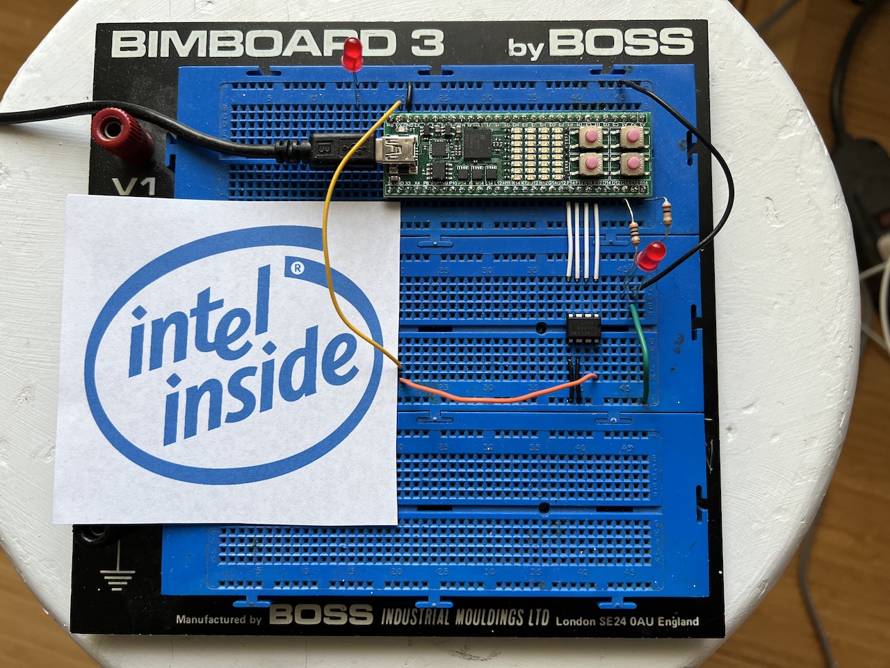
Pictures
Source code
https://github.com/mikeakohn/intel_8008
Copyright 1997-2026 - Michael Kohn
