W65C832 In An FPGA
Posted: October 16, 2024
Introduction
Back in the 80's, the Western Design Center (WDC) created a 16 bit version of the 6502 CPU called the W65C816. I believe it was created for the Apple IIgs computer, although it was also used in the Super Nintendo. It appears they had a data sheet for a 32 bit version of the chip called the W65C832. I decided to do a Verilog version of it in an FPGA.
I updated naken_asm so it has a .65832 directive that allows immediate values for things like lda and such to have a .l modifier so it can do 32 bit values now.
The instruction set is able to access 16MB of RAM. The FPGA itself has a small amount of block RAM that this w65c832 core uses as 4k of RAM at the bottom of memory (for zero / direct page), 4k as ROM, and 4k as pages for a Winbond W25Q128J flash chip or 512 byte pages for an SD card. More on that further on this page.
The Verilog source code is available on GitHub and builds with the regular opensource FPGA tools: yosys, nextpnr-ice40, icepack, and iceFUNprog. I recently added support for the Tang Nano 20k board (should work with the 9k model too) using the same basic set of tools: yosys, nextpnr-himbaechel, gowin_pack, and openFPGAloader. The Makefile shows how they are both built. Hopefully a bigger project will come from this.
Joe Davisson helped me test and debug the core (he fixed a few bugs himself) and created a really wicked graphics demo in assembly with this core along with an XMODEM bootloader so that programs can be uploaded over a UART instead of built into the Verilog: Joe's W65C832 demo.
Related Projects @mikekohn.net
| FPGA: | FPGA VGA, Nexys2, Glow In The Dark Memory, Intel 8008, F100-L, RISC-V, x86 / 68000, MIPS, MSP430, PowerPC, W65C832, Apollo 11, PDP-11 |
65C832
The chip itself has 3 registers still:
A (8/16/32 bit accumulator)
X (8/16/32 bit index x)
Y (8/16/32 bit index y)
Along with some more internal registers of the 6502 and some newer 65C816 registers:
SP  (16 bit stack pointer)
PC  (16 bit program counter)
DR  (Direct Register  - 65C816)
DRB (Data Bank Register - 65C816)
PRB (Program Bank Register to extend PC to 24 bit - 65C816)
There's a status register (called P for some reason):
 P: 7 6 5 4 3 2 1 0
    N V M X D I Z C

N negative (set if bit 7 of the result is set)
V overflow
M
X / break
D decimal
I interrupt disable
Z zero     (set if ALU result is 0)
C carry    (set if ALU result requires bit 8)
There are two other 1 bit registers called E16 and E8 that pick what mode the CPU is operating in. They can't directly be accessed, but instead are accessed through an XCE instruction, which acts differently depending on if the CPU is in 8 bit emulation mode or not.
M flag sets the size of A and memory fetches.
X flag sets the size of X and Y.


    // E16  E8   M   X    A    X,Y    Mode
    //  0    0   0   0   16    32     W65C832 Native
    //  0    0   0   1   16     8     W65C832 Native
    //  0    0   1   0    8    32     W65C832 Native
    //  0    0   1   1    8     8     W65C832 Native
    //  0    1   0   0   32    32     W65C832 Native
    //  0    1   0   1   32     8     W65C832 Native
    //  0    1   1   0    8    32     W65C832 Native
    //  0    1   1   1    8     8     W65C832 Native
    //  1    0   0   0   16    16     W65C816 Emulation
    //  1    0   0   1   16     8     W65C816 Emulation
    //  1    0   1   0    8    16     W65C816 Emulation
    //  1    0   1   1    8     8     W65C816 Emulation
    //  1    1   1  BRK   8     8     W65C02  Emulation
E16 and E8 change the emulation mode. At startup, the all 3 flags are 1 while BRK is ignored. To switch from W6502 emulation to W65C816 emulation:
    clc
    xce
While in W65C816 mode, the xce (Exchange C with E8) instruction becomes the xfe (Exchange C with E8 and Exchange V with E16) instruction. So to change to W65C832 mode while in W65C816 mode:
    sec
    clv
    xce
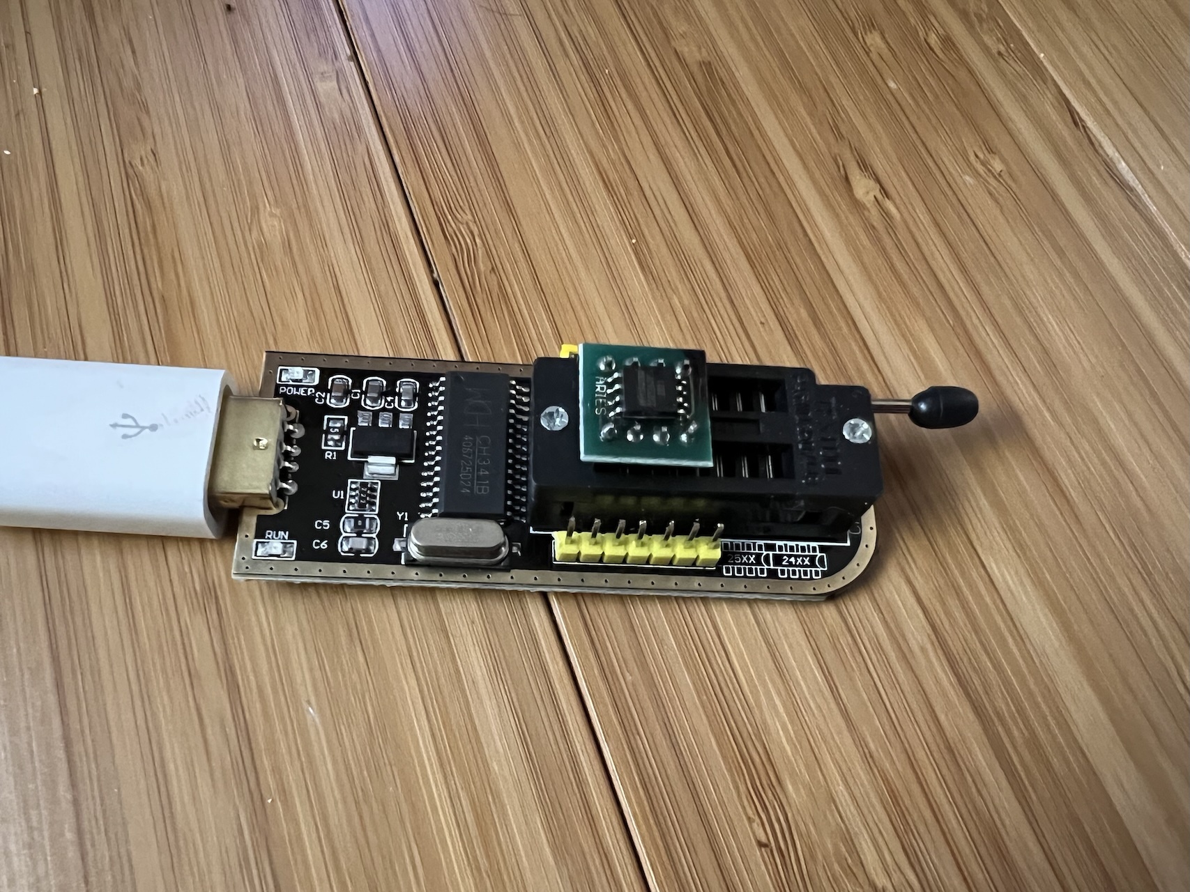
Winbond W25Q128
To add a lot more ROM area, this implementation can use a Winbond W25Q128 16MB flash chip. The core uses the memory similar to virtual memory. Accessing any memory address 0xc000 or above will trigger the CPU to pause while 4k of flash is transfered from the flash chip to RAM. At that point that 4k page is immediately accessable. If a memory location is read that isn't in the currently loaded page, the CPU again will pause and the next page will be read in.
To program the flash, a CH341A along with a program called flashrom was used to tranfer a .bin file to the chip. The commands used to write the out.bin to flash and then read it back to a rom.bin file to make sure it works:
flashrom -p ch341a_spi -c W25Q128.V..M -w out.bin
flashrom -p ch341a_spi -c W25Q128.V..M -r rom.bin
Here is a picture of the CH341A programmer with the flash ROM in the ZIF socket:
Any memory below 0xc000 in the flash is ignored, but anything 0xc000 and above is mapped directly into the CPU. To access memory location 0x20003 in the flash memory, the following code can be used:
  lda.b #2
  pha
  plb
  lda 0x0003
The instructions set the accumulator to 2, pushes it to the stack with pha, pulls it from the stack to the dbr (data bank register) with plb, and uses lda 0x0003 to pull from the effective address of 0x20003.
It could be possible to make the CPU write back pages into the flash ROM when they are paged out, but that doesn't seem very practical.
Micro SD Card
Recently I decided to replace the Winbond chip with just an ordinary SD card. Since the standard page size on an SD card is 512 bytes, the page size here is reduced to 512. It's possible in the future this could be bumped up to 4096.
To get a feel for SD cards again, I created a small sample program in the naken_asm repository (sd_card.asm and sd_card_sdhc.asm) that does the absolute minimum to read a sector from a smaller SD card using an MSP430. Those steps were then translated to Verilog in the sd_card.v module.
For the absolute minimum to read from a 2GB card:
With /CS high, send 10 bytes.

Pull /CS low and send reset (CMD0): 0x40, 0x00, 0x00, 0x00, 0x00, 0x95
(Reponse should be 0x01)

Repeat until reponse is 0x00:
  Pull /CS low and send init (CMD1): 0x41, 0x00, 0x00, 0x00, 0x00, 0x00

To read sector starting at address 0x00000200:
  Pull /CS low and send read (CMD17): 0x51, 0x00, 0x00, 0x02, 0x00, 0x00
  Keep reading bytes until response is 0xfe, then read 512 bytes, and
  then another 2 bytes for a checksum.
For reading a sector, the argument (the 4 bytes after the command byte) are the address of the start of the sector. This 32 bit value must be a multiple of the size of the sector. In the case of sd_card.v it's assume to be a multiple of 512.
To read from an SDHC card (more then 4GB):
With /CS high, send 10 bytes.

Pull /CS low and send reset (CMD0): 0x40, 0x00, 0x00, 0x00, 0x00, 0x95
(Reponse should be 0x01)

Pull /CS low and send xxxx (CMD8): 0x48, 0x00, 0x00, 0x01, 0xaa, 0x87
(Reponse should be 0x01)

Repeat until response is 0x00:
  (CMD55)  0x77, 0x00, 0x00, 0x00, 0x00, 0x00
  (ACMD41) 0x69, 0x40, 0x00, 0x00, 0x00, 0x00

To read sector starting at address  0x00000200 (parameter is page number):
  Pull /CS low and send read (CMD17): 0x51, 0x00, 0x00, 0x00, 0x01, 0x00
  Keep reading bytes until response is 0xfe, then read 512 bytes, and
  then another 2 bytes for a checksum.
This part started with a 2GB card since the code was a little simpler. Since 2GB cards are harder to find now, an sd_card_sdhc.v was created.
Memory Map
This implementation of the W65C832 has 4 banks of memory. If there is a Winbond W25Q128JV, Bank 3 and all memory above up to 16MB will be paged in (and out) of RAM 4k at a time.
Bank 0: RAM (4096 bytes)
Bank 1: ROM (4096 bytes from rom.txt)
Bank 2: Peripherals
Bank 3: Micro SD Card / Winbond W25Q128JV Flash (filling up to 16MB).
On startup the chip will execute code from Bank 1. If the program select button is pushed on reset code will start from location 0xc000 in Bank 3.
The peripherals area contain the following:
0x8000: input from push button
0x8001: SPI TX
0x8002: SPI RX
0x8003: SPI CTRL
0x8008: ioport0 output (in my test case only 1 pin is connected)
0x8009: MIDI note value (60-96) to play a tone on the speaker or 0 to stop
0x800a: iport1
0x800b: UART TX buffer
0x800c: UART RX buffer (reading clears out rx_ready)
0x800d: UART CTRL - bit 1: rx_ready, bit 0: tx_busy
The UART can be accessed through a cheap USB-UART cable. The cable must have logic levels of 3.3v only. There is a picture below showing how it's connected.
Joe Davisson created a bootloader over the UART (works with EasySXB too) so changing the software doesn't require reprogramming the FPGA or a flash/eeprom chip.
Explanation
Even with just the 65C816, the register modes (8 or 16) bit can be a challange to work with. When working on the PANCAKE-ROM project, I got bit by mixing up what mode the CPU was in while writing some memory locations. The memory manipulation was assumed to be in 16 bit mode, but it was 8 bit. The 65C832 makes this even more rough.
While working on the test/lcd.asm, which blinks an LED and draws a Mandelbrot on an LCD display when a button is pushed, a few times I would forget when using immediate to use the proper modifier:
0x0000: a9 05            lda.b #0x0005
0x0002: a9 05 00         lda.w #0x0005
0x0005: a9 05 00 00 00   lda.l #0x0005
If the CPU is in 8 bit mode and the lda.l is used, it will read in only 0xa9 and 0x05 to load A and then execute the 0x00 part (brk) of the immediate that it didn't read in.
I also got bit when trying to load the P (status register) into A. While in 32 bit mode I did:
php
pla
This pushed 1 byte for the P register and popped 4 bytes into A.
When disassembling code, the disassembler never knows what mode the CPU is in (8, 16, 32 bit) so it makes doing a disassembly of 65C816 and 65C832 code pretty much impossible.
Subroutines also have to be sensitive to what mode the CPU currently is in. In lcd.asm, subroutines would push the P (flags) register and pop status when leaving the subroutine. The bad part is e16 and e8 are not a part of the flags so saving those off is a bit more complex. With the 65C816 this wasn't as much of a problem, once out of 6502 emulation mode, both A and X/Y can be in all modes with just sep and rep, no need to mess with e8. Not so much in 65C832.
Inside the 65C832 Verilog, I got bit by some instructions reusing the opcode space of others. So, every 8 bit opcode in the 6502 can be broken up into 3 pieces: aaa bbb cc. The first 3 bits (aaa) are kind of the operation, the bbb part is typically the addressing mode, and cc kind of separates out different types of opcodes. One instruction I got bit by was the "bit" instruction. If cc is 00 then if the operation (aaa) is 001, it's a "bit" test instruction for addressing modes immediate, zero page, absolute, zero page with x, and absolute with x. What I didn't realize (until I spent too long on a bug in lcd.asm) is that bit #imm overlaps with c=01, aaa=001 which is supposed to be the sta instruction. If it's an sta instruction and the addressing mode bbb=010 (immediate) it's kind of useless so the bit #imm (100_010_01 or 0x89) was placed in that opcode space.
The test/lcd.asm that draws a Mandelbrot on an LCD display was ported from the F100-L FPGA version. It uses fixed point math of 6.10 (6 bits integer and 10 bit fraction) so most of the Mandelbrot code runs in 16 bit accumulator mode. It switches to 32 bit mode when doing the multiply and back to 16 bit after shifting the result right 10 times. The code exercises quite a bit of the instruction set including stz.
The 65C832 Mandelbrot takes around 1m8s to generate.
Picture
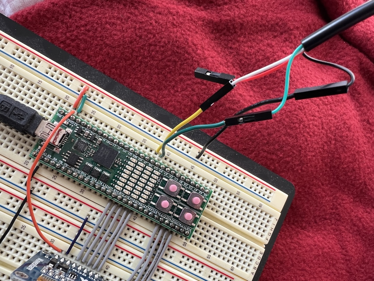
The picture above shows how to connect a UART cable. To prevent damage to the FPGA, this must be a 3.3v logic cable. The 5v red wire is not needed and left unconneted. The green wire is TX transmit and is connected to G3 on the FPGA (the RX receive pin). The white wire is RX receive on the USB side and is connected to H3 (the TX transmit pin).
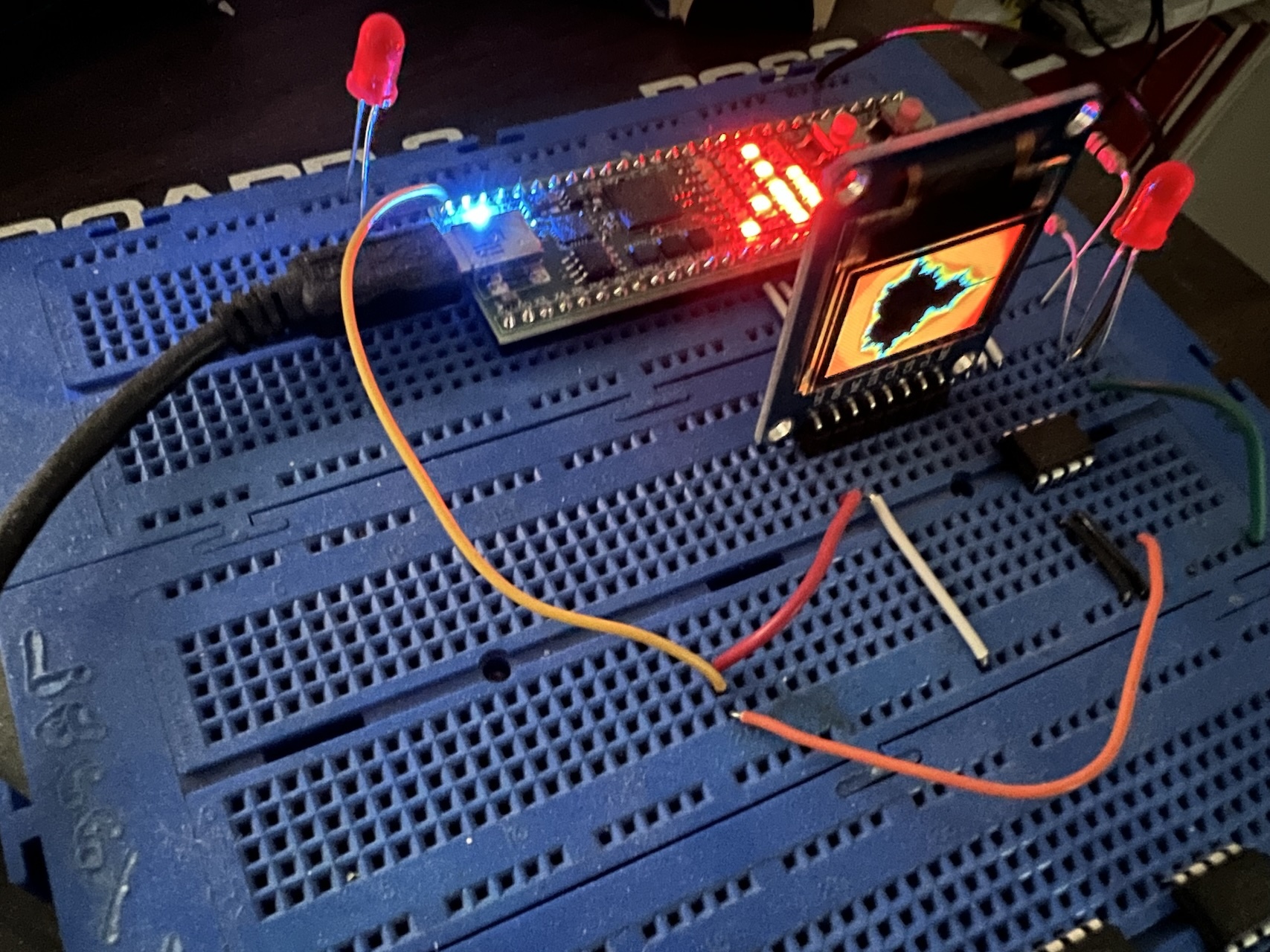
This is the IceFUN with the W65C832 verilog code in it running the lcd.asm demo.
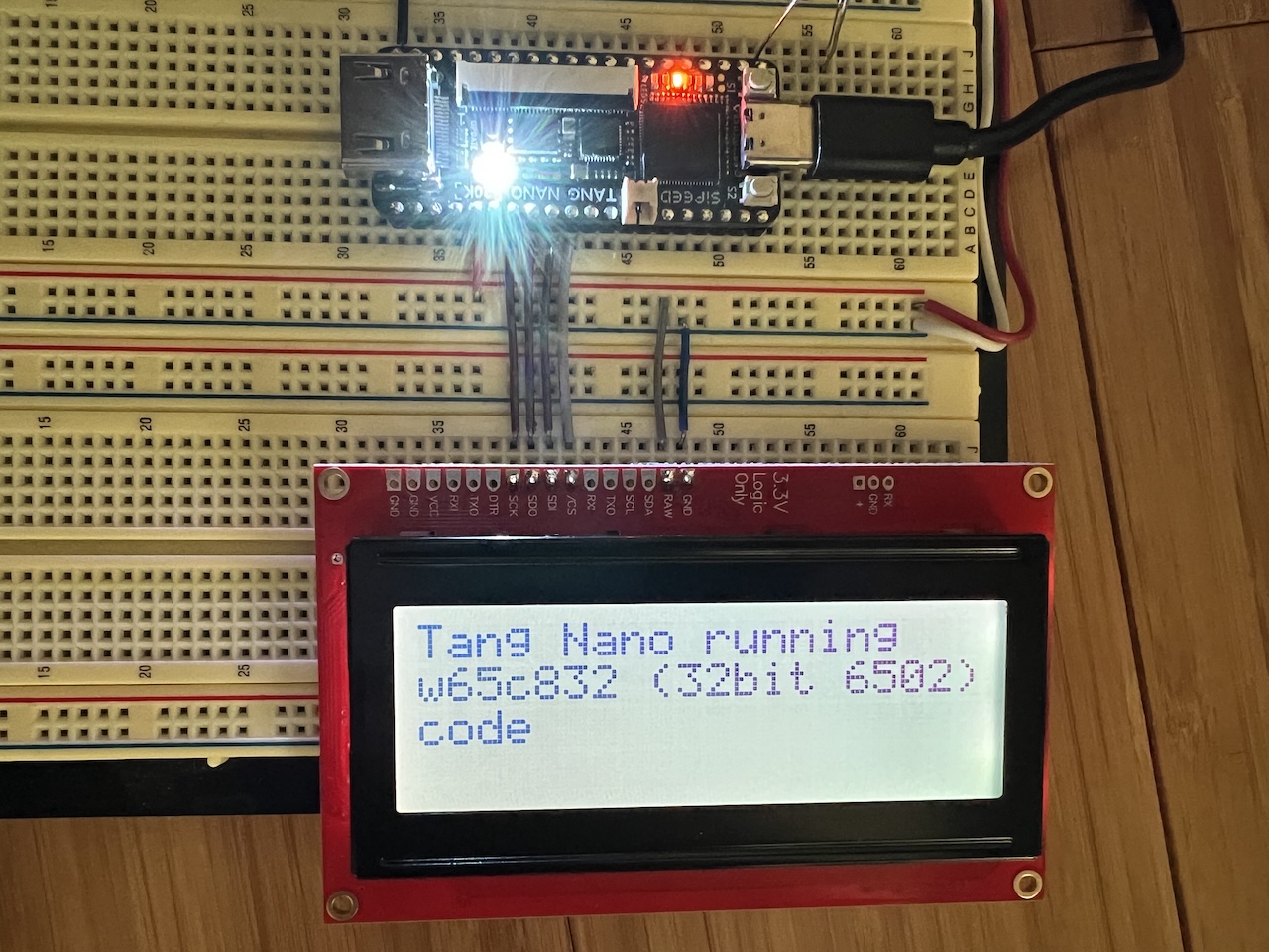
Here's a Sipeed Tang Nano 20k with the same (slightly modified for the board) w65c832 core. The program running on the core writes out to a SparkFun LCD display. The core is still built on the same opensource tools, but uses some of the specific tools for the GoWin chip: yosys, nextpnr-himbaechel, and openFPGAloader.
After having trouble building the opensource tools for the Tang Nano I created this short document showing the steps to build it in docker: Open-Source FPGA Development.
Differences
As of this writing, there are a few things that need polishing or needs to be implemented. These will probably eventually be done:
- Instruction timings don't match the spec.
- Decimal mode isn't implemented.
- 6502 Emulation mode allows newer instructions to work.
There might be others I'm forgetting.
Improvements
At some point before working on this, I had some other ideas of doing a 32 bit 6502 that didn't use the rep/sep model on some flags to change the width of the registers. One idea was more similar to the Intel x86 model. The idea would be for the CPU to interpret all instructions as 6502. So it's 100% 6502 code compatibile, but when the width of an instruction should be 16 or 32 bit (or even 64 bit) there would be a 1 byte prefix infront of that instruction to change the register size. It would basically make using the CPU in 16 or 32 bit mode 1 byte longer, but at least the code can be disassembled and there's less of a chance of accidentally using a register in the wrong size.
At some point I could change this core to work this way...
Source Code
git clone https://github.com/mikeakohn/w65c832.git
Copyright 1997-2026 - Michael Kohn
