Glow In The Dark Memory
Posted: April 11, 2022
Introduction
Here's a project to show how glow in the dark stickers could be used as RAM. The idea is to have 1 byte of RAM made of up 8 glow in the dark stickers. Each bit can be charged up (put into a 1 state) by a white LED and read back with a phototransistor. The array of glow in the dark stickers can be interfaced to the memory bus of a computer through an FPGA.
The FPGA devkit I used is an iceFUN FPGA board and the CPU of choice is the Wester Design Center MENSCH SBC. The reason for the iceFUN was because it's a super cheap board with a lot of pins with a ton of features, most notably a grid of LEDs that made debugging so much easier. Really, this is a beautiful board. The MENSCH board was perfect for this too because it exposes the data and address bus along with other signals to make this project possible.
Because the FPGA with stickers are on the MENSCH's memory bus, any software written to access location 0x200 with regular 6502 / 65C816 instructions have no idea they are accessing stickers rather than regular RAM:
lda #0x55
sta 0x200  ;; Sets stickers to 0101_0101.
lda 0x200  ;; Reads the values of stickers back into A.
This project really has no practical purpose. It's pretty much as useful as the PANCAKE-ROM and Tin Can Phone Modem. It is maybe an interesting example of how to use the data / address bus from a CPU to an FPGA at least.
There is a detailed explanation below along with a video, pictures, and a link to the git repository.
Video
Pictures
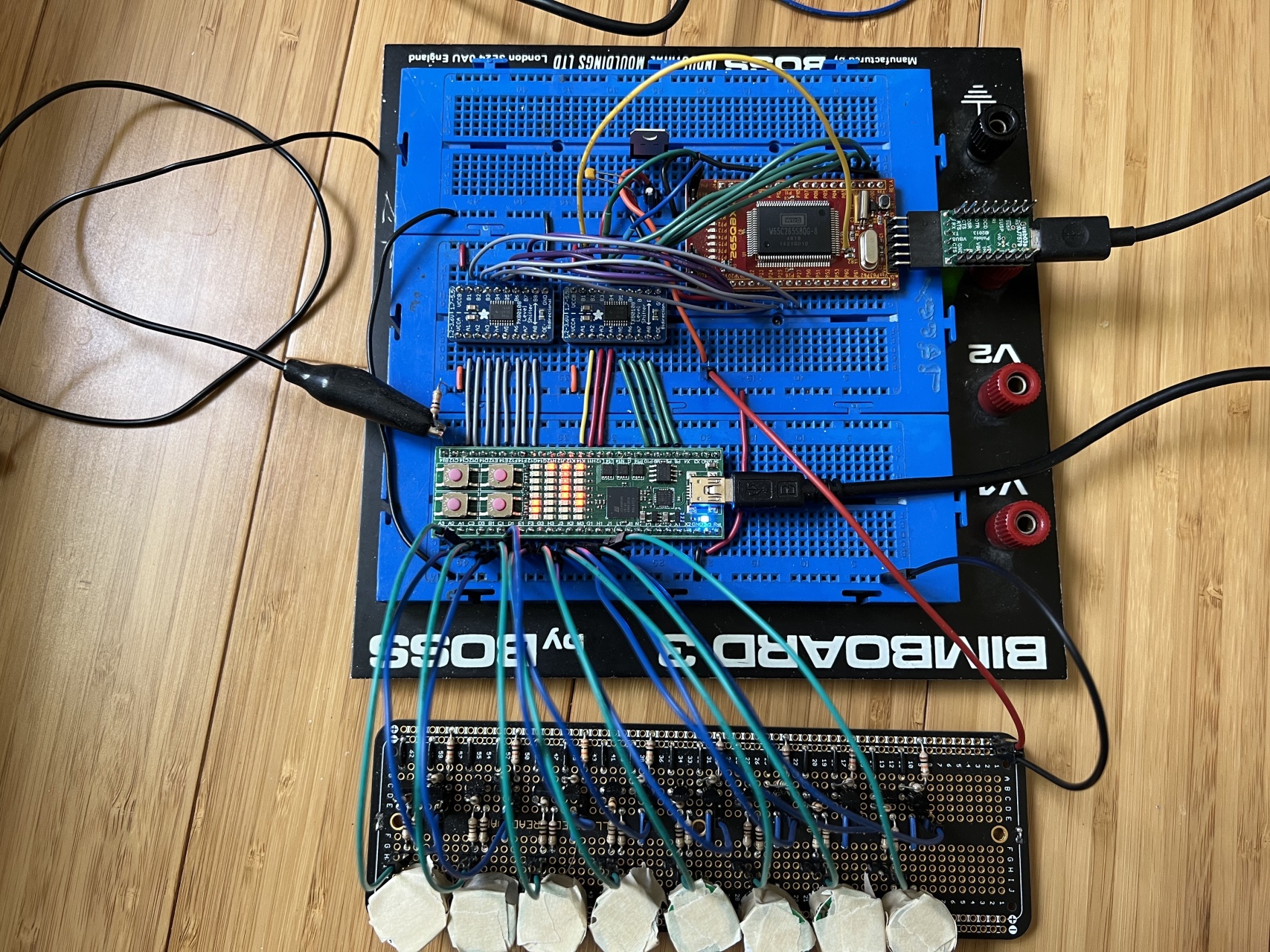
The picture above shows the entire circuit. Starting from the bottom is the board that has the 8 bits of glow in the dark stickers. This board is connected to the iceFUN FPGA board above it. The FPGA is connected to the WDC MENSCH board by 8 gray wires (the databus), a yellow wire (the bus enable BE signal), a red wire (the PHI2 clock signal), another red wire (the WEB write enable signal), and 4 green wires (4 bits of the address bus which I didn't end up using). Between the FPGA and the MENSCH are 3.3v to 5v level shifters.
The LEDs on the in the FPGA starting from the left side show the current value of the 1 byte of data (currently 01100000), the value last sent on the databus (00000001), signal data (WEB=1, PHI2=<blinking>, BE=<blinking>, busy=1, reset=1), and on the far right state=1 (waiting for glow in the dark stickers to erase) along with some other debug info.
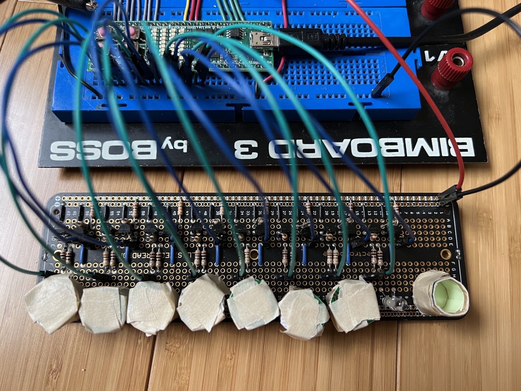
Above is a close up of the glow in the dark sticker portion. On the right side, one of the "caps" is removed exposing the white LED (on the left) and a phototransistor. The entire inside of the cap has glow in the dark material, including on the side wall. Without the side wall tape, each bit wasn't holding its value for long enough.
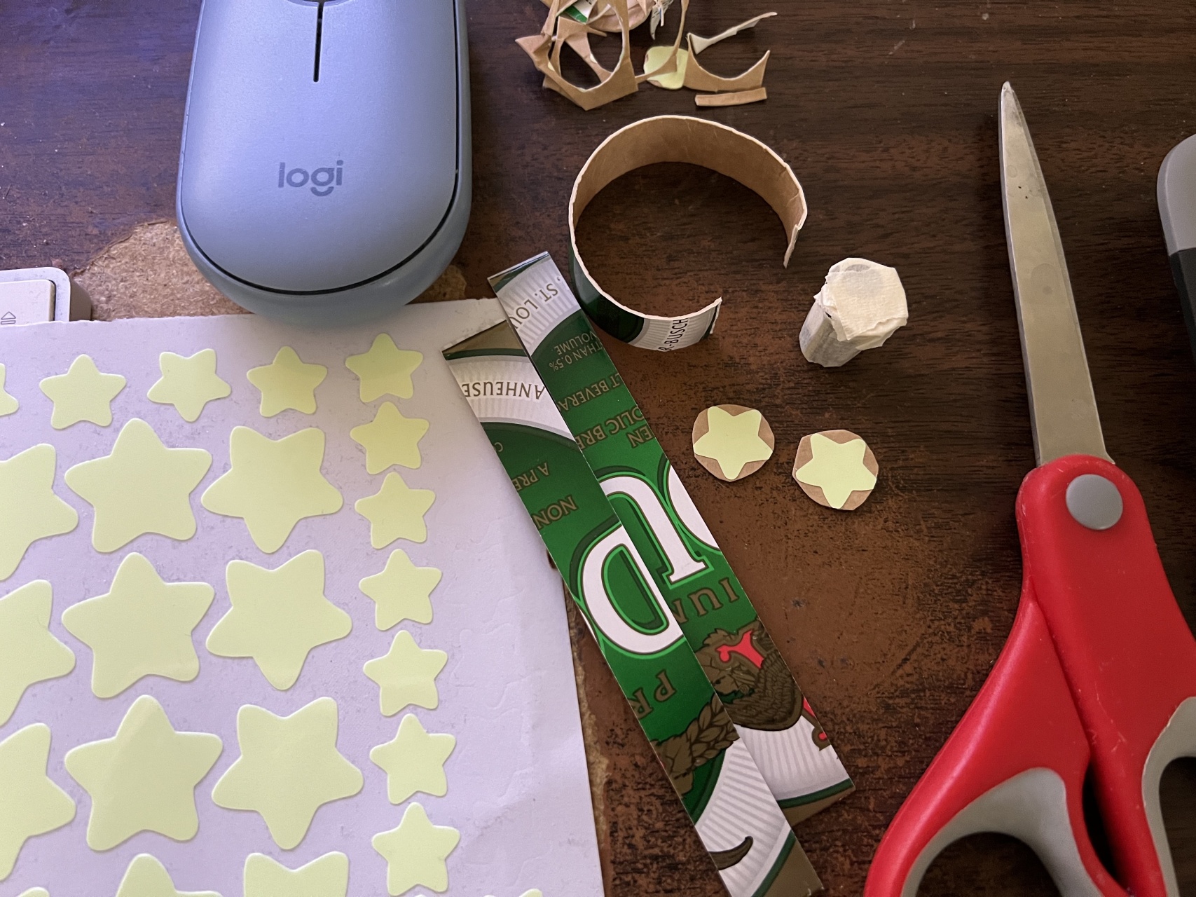
Here's a picture of the stickers along with the cardboard used to make each glow in the dark bit.
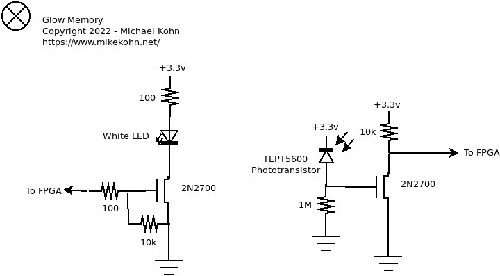
This is the schematic for each glow in the dark sticker.
Explanation
The whole concept is similar to the way DRAM works, but instead of capacitors to charge up and read from, some glow in the dark stickers were used. Since the glow in the dark material fades over time, the system has to go through a refresh cycle to replenish the value on lit bits similar to the way DRAM does except obviously much slower.
The MENSCH SBC
The MENSCH SBC was just the perfect board for this project. The board exposes the address and data bus on the bottom headers along with the WEB (write enable) and PHI2 (the W65C265's clock signal) on top of the board. The BE (bus enable) signal was also needed to halt the bus when the FPGA is erasing the memory (basically just waiting for the glow of the stickers to die out) or writing data to the stickers. Unfortunately, BE was not exposed so easily. I was forced to solder a wire directly infront of the surface mount pull-up resistor on the board. One thing to note, hooking up an FPGA to the MENSCH SBC on the memory bus doesn't require the BE signal unless the FPGA needs to pause the CPU before it can return the requested information on the data bus.
The BE signal ended up being a bit awkward... it's used for multiple functions. I used some smaller FPGA boards, the iceBlips, to figure out how to get the BE signal working. The way I got it working, which according to the datasheet seems like I did it wrong, was by pulling BE low while PHI2 was high, but letting BE go back high whenever PHI2 is low. When the CPU is free to run code, BE is left high.
The MENSCH exposes 16 bits of the address bus and I had wired up 4 of those bits. When I did the test of this with the iceBlips FPGA board, I was using the address bus so 15 memory locations would be hardcoded ROM and 1 memory location would be writable. Those 16 locations of data would be mirrored throughout that memory region. When I got the iceFUN I decided to ignore the address bus altogether and just mirror that one byte throughout the memory region.
The MENSCH board is also supposed to have the ability to run at 3.3v, but I just couldn't get that working so I kept it at 5v (powered over USB by a Pololu USB-to-Serial adapter) and used 8 channel TXB0108 level shifters from Adafruit.
Anyway, I did at some point consider an 8051 if I couldn't get this working since it too exposes an address / databus and it could have got its clock source from the FPGA, so the FPGA could just stop clocking when the memory was busy, but this worked.
Verilog
This is the part of the project I really struggled with the most. I really haven't done too much with FPGAs before.
So to start with, since I didn't want to use official tools from Lattice, I compiled the following OpenSource tools:
https://github.com/YosysHQ/icestorm.git
https://github.com/YosysHQ/nextpnr.git
https://github.com/cliffordwolf/yosys.git
https://github.com/devantech/iceFUNprog.git
I did run into some problems compiling nextpnr. I had to do the following cmake command:
cmake .. -DBUILD_PYTHON=0 -DARCH=ice40 -DICESTORM_INSTALL_PREFIX=/source/icestorm
The Verilog code consists of two modules: glow_memory.v and ram.v. The ram.v module contains a state machine for dealing with reading and writing the stickers:
// State 0: Memory is readable (optimized for zero).
// State 1: Erase cycle.
// State 2: Move to state 3.
// State 3: Write cycle.
// State 4: Move to state 5.
// State 5: Memory is readable (non-zero).
When the FPGA is in state zero, either reset is held low or the current value of the stickers is supposed to be 0. In this state there isn't a need for a refresh cycle.
State 1 is the erase cycle where the FPGA sits idle (holding the busy signal high so the glow_memory.v will halt the CPU) until all the stickers read back as 0.
State 2 is just a transistion state for moving to state 3. Maybe could have skipped that, but it only hurts by a CPU cycle or so.
State 3 is the write state. In this state any LEDs that need to be turned on to charge the stickers are lit. This continues for 4 million CPU ticks from PHI2.
State 4 is also a transition state and maybe not needed.
State 5 is in a read state. The FPGA will stay in this state for about 8 million CPU ticks and will then go back to state 3 to refresh the stickers.
If the WEB signal goes low, data is read from the databus on the transition back high and the FPGA goes to state 3 to store that data into stickers.
Timing
One big question was how long to keep the white LED on to charge the glow in the dark stickers and how long will it last before it needs to be refreshed. To get an idea how long each cycle could be, I started out with a simple MSP430 circuit / program on a breadboard.
There ends up being a lot of variables which affect these timings:
- Size of the resistor on the detector circuit.
- Brightness of the charging LED.
- How much glow in the dark material there is.
- Distance from the LED / Phototransistor to the stickers.
The numbers of 4 million PHI2 ticks to charge and 8 million PHI2 ticks before the next refresh were chosen based on the timing that appeared to work for the MSP430. It does pick up some errors sometimes but for the most part appears to work.
Source code
https://github.com/mikeakohn/glow_memory
Copyright 1997-2026 - Michael Kohn
