Ferranti F100-L In An FPGA
Posted: January 15, 2024
Introduction
Back in the mid-1970's, there was a 16 bit chip developed called the Ferranti F100-L. It seems it was used by the European defense industry, so I thought this would be really cool to add to naken_asm. After adding the assembler I thought it might be fun to do the whole CPU Jurasic Park thing and ressurect the chip from the dead with an FPGA.
The project was done by copying the source code from the Intel 8008 project, changing the memory bus to handle 16 bit words, and replacing the core instruction decoding with F100-L.
Again, the FPGA devkit used is an iceFUN FPGA board (Lattice iCE40-HX8K) along with the opensource IceStorm tools.
The core itself is finished and there is a video of it generating Mandelbrots and by taking advantage of FPGA hardware to accelerate the process. There is also Java Grinder support for the F100-L now which is demo'd in the video. I have some more plans for this chip, so I consider this project still open.
Below is a video, bigger explanation, and a link to the Verilog source code.
Related Projects @mikekohn.net
| FPGA: | FPGA VGA, Nexys2, Glow In The Dark Memory, Intel 8008, F100-L, RISC-V, x86 / 68000, MIPS, MSP430, PowerPC, W65C832, Apollo 11, PDP-11 |
Video
The first part of the video demonstrates loading a program off of the EEPROM into one of the RAM areas. The program generates a Mandelbrot in software. Since the Mandelbrot takes 70 seconds to generate, most of the generation was cut out of the final video. When the user button is pushed a second time, a Mandelbrot is generated in hardware with a Mandelbrot peripheral. The video also demonstrates moving a servo with a built in servo peripheral. Last, there is a demonstration of a program written in Java that plays a song.
YouTube: https://youtu.be/CrETRt_e1Ko
The four buttons are:
- Upper right: reset
- Upper left: program select (holding down on reset loads from EEPROM)
- Lower right: halt
- Lower left: user button
The rows of LEDs are used for debugging. The rows of LEDS (from left to right) are:
- Lower 8 bits of accumulator (A)
- Upper 8 bits of accumulator (A)
- Lower 8 bits of program counter
- CPU state register (fetch, decode, halt, etc)
F100-L
This chip was kind of a pain to find any information on. There was one really good site that I used to create the assembler and the Verilog: The F100-L Instruction Set along with a PDF that sometimes disagreed with this page. Unfortunately, doing a web search for F100-L mostly brings up information on Ford trucks.
So when I started this core, I had just finished implementing a minimalist RISC-V core in an FPGA (code complete, but not tested yet... a lot did change since then). So I was able to use things I learned from that project that I didn't know when I did the Intel 8008 core. I also took some new knowledge from working on this back to the RISC-V and the Intel 8008.
The biggest thing that hit me when doing the F100-L, and comparing it to the RISC-V, is that even though the bits of the opcodes of the F100-L are pretty nicely organized, this is *NOT* a RISC CPU. And when coding the Verilog, it was rough. A great example is the CAL instruction. This instruction is used to call a function while storing the return address and condition register on the stack. The stack pointer on this chip isn't a register, it's stored in location 0. So the steps to do this:
- Read location 0 into a temporary stack pointer register (lsp).
- Store the PC into the address of lsp+1.
- Store the CR into the address of lsp+2.
- Add 2 to lsp.
- Write lsp back to location 0.
Not sure if I did this the most efficient way, I still feel like a n00b with FPGA/Verilog, but I did each memory access with 2 cycles (2 states in the CPU state machine). It was painful.
Test Programs
There are a few small programs in the test/ directory, the two that actually do something are blink.asm and lcd.asm. The lcd.asm program writes out to SPI and creates Mandelbrots while blink.asm just blinks an LED. They assemble with naken_asm which can support older F100-L code, but has a newer syntax that makes the code easier to read. The samples all use the newer syntax. If the programs are loaded onto EEPROM, they also must change the .org value so they can be run from memory location 0x6000.
Servo Control
This design also has a servo control peripheral. It supports up to 4 channels using 4 peripheral addresses. Setting the address to a value between 12,000 to 24,000 will create a pulse on that output pin between 1ms and 2ms which would tell the servo how far to the left or right to be rotated.
Java Grinder
Support for the F100-L was added to Java Grinder. In the samples directory, an IceFunDemo.java program was added to play a little song using the iceFUN speaker. An API was added specifically for the iceFUN board that has support for both the speaker and servo control. SPI support also works, and the LCD display is used as a demo for that. The same program that runs on the iceFUN with F100-L runs on the iceFUN as a RISC-V chip (after the .class files are further compiled with Java Grinder). Write once, run on iceFUN.
This was a massively weird architecture to add to Java Grinder. The F100-L doesn't have "pointers" as registers, but instead memory locations 1 to 255 can hold an address to use as a pointer using the "lda A, [address]" addressing mode. It's similar to the 6502's indirect addressing. Because of this, variables have to be stored between memory location 1 to 255. Since memory location 0 is the stack pointer and no instruction has access to it as a pointer, the Java Grinder frame stack and Java computation stack are separated from the CPU stack. The CPU stack starts at location 0x100 and is only up to 16 calls in length (32 words). All global variables along with the Java call stack has to sit between location 4 and 254. Location 255 is used as a temporary pointer.
There is more information on the F100-L in the GitHub repo for this project.
Mandelbrots
The main test program which is stored on the EEPROM in the demo is the test/lcd.asm program that is loaded onto an EEPROM. The program has functionality to blink an LED, initialize an LCD over SPI, clear the screen, generate a Mandelbrot in software, and generate a Mandelbrot using a special Mandelbrot peripheral. The Mandelbrot peripheral works by having memory locations where a real value (16 bit fixed 6.10) and an imaginary value can be loaded. Another MANDELBROT_CTL register in the peripherals memory space can be strobed to start the calculation and flag when the result is ready. One final memory location has the result of the calculation (a number between 0 to 15). The result is the software Mandelbrot takes about 1 min 10 seconds to generate while the hardware version is around 1 second.
The hardware Mandelbrot code is in the mandelbrot.v Verilog module and I was able to copy it to the RISC-V repo and simply remove it from the RISC-V peripherals and give the risc.v module access through a custom instruction.
Memory Map
The memory map for this project consists of 4 banks:
- Bank 0: 0x0000 RAM (2048 words)
- Bank 1: 0x2000 ROM (2048 words, an LED blink program from blink.asm)
- Bank 2: 0x4000 Peripherals
- Bank 3: 0x6000 RAM (2048 words)
On startup, by default the code in bank 1 (hardcoded by the file rom.v) will run. To run code starting at location 0x6000, the push button connected to C6 on the FPGA should be held down while the system is being reset. The code needs to have .org set properly for location it will run in.
Every address in this CPU is actually 16 bit, not the typical 8 bit. So each RAM bank, even though it's 2048 words, it's actually 4096 bytes. Oddly, the instruction set was limited to 15 bit addressing, even though it really could have been 16 bit. I was tempted to make this core able to do 16 bit, but decided to just stick with the design of the original chip.
The peripherals bank contains the following locations:
- 0x4000: input from push button
- 0x4001: SPI TX buffer
- 0x4002: SPI RX buffer
- 0x4003: SPI control: bit 2: 8/16, bit 1: start strobe, bit 0: busy
- 0x4008: ioport0 output (in my test case only 1 pin is connected)
- 0x4009: MIDI note value (60-96) to play a tone on the speaker or 0 to stop
- 0x400a: ioport_B output (3 pins)
- 0x400b: mandelbrot real value
- 0x400c: mandelbrot imaginary value
- 0x400d: mandelbrot control: bit 1: start, bit 0: busy
- 0x400e: mandelbrot result (bottom 4 bits)
- 0x4010: servo_0 value (2ms = 24,000, 1ms = 12,000)
- 0x4010: servo_1 value
- 0x4010: servo_2 value
- 0x4010: servo_3 value
EEPROM
There's special code inside the f100l.v that if the program button is held down during reset, the code from an AT93C86A EEPROM is loaded into 0x6000 region of RAM and executed. To program the chip, a TL866-II Plus universal programmer is used along with the opensource software minipro.
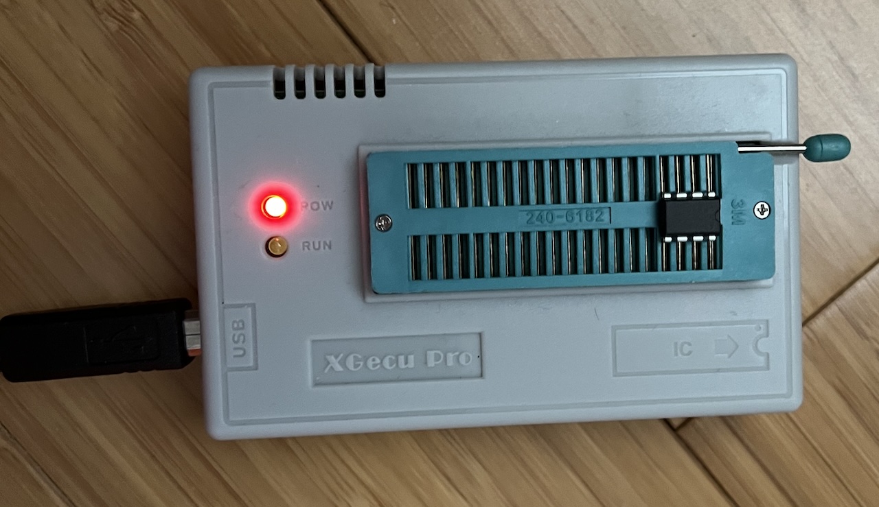
./minipro -p "AT93C86A(x8)" -s -w lcd.bin
Testing And Debugging
This project really needs a program that tests every instruction and does a halt if there is a problem. At some point I could add that, but I don't have the time right now.
Improvements
Some of the instructions I think can be executed in less cycles, in a single state instead of multiple. It makes the code a little harder to read I think, so I'll probably be leaving the code as it is.
Pictures
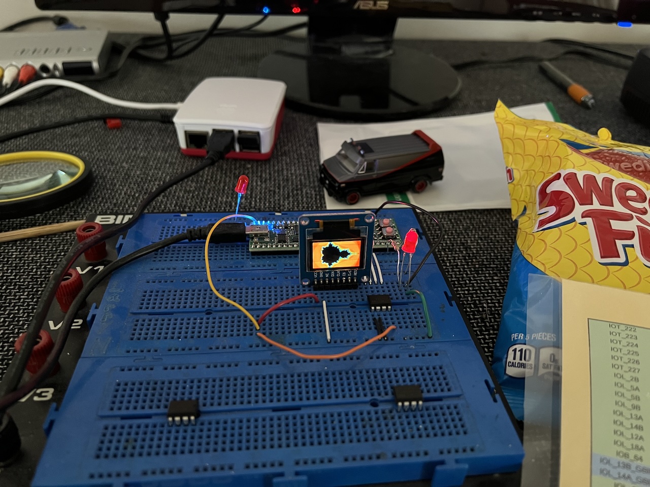
Here's the iceFUN board showing a Mandelbrot. It's connected to a Raspberry PI 5 which because all the FPGA tools are opensource can also be used for building the project.
Source code
https://github.com/mikeakohn/f100l_fpga
Copyright 1997-2026 - Michael Kohn
