RISC-V FPGA
Posted: January 15, 2024
Updated: January 26, 2025
Introduction
Here's a project that demonstrates the advantage of having an opensource instruction set (RISC-V) along with the power of being able to wire an FPGA into one. This project implements a minimal RISC-V core in an iceFUN FPGA board. While having a license-free instruction set is nice, it also opens up the possibility to implement custom instructions, in this case a Mandelbrot instruction. The video below demonstrates the speed improvement that can be gained by optimizing it in hardware with a custom instruction.
Java support for RISC-V was added to Java Grinder along with an iceFUN API for it. There is a demo of the sample Java program called IceFunDemo.java (which will also compile and run without changes on F100-L) in the video below. All of the sample programs in the test/ directory of the git repo can be assembled with naken_asm.
The project started as a fork of the first CPU core I worked on, an Intel 8008. I again used all the opensource IceStorm tools to develop the code. I actually took a break in the middle of this to complete an F100-L CPU core and backported some cleanup / fixes from that project into this one. In the explanation below, there will be some comparisons between the 3 projects. I'm still pretty new to this stuff and other than asking coworkers questions occasionally I'm pretty much learning on my own. Therefore there might be some odd stuff in the code so beware to anyone trying to learn from this project.
More recently, I also did speed / code density comparisons of this RISC-V core against similar x86 and 68000 cores.
Joe Davisson also created a bootloader for this core. It uses XMODEM so programs can be uploaded into into the core using a term program like MiniCom. I'll post a binary so anyone can buy the IceFun board and just use their simple uploading software to load it. No need to build the Verilog from source code. More info about that on his website: XMODEM Bootloader
Update July 3, 2024: I copied the riscv.v source file and created a ciscv.v Verilog file which has some extra instructions that ARM64 has to see if performance could be improved in situations. There is a writeup on that towards the bottom of this page.
Update Jan 26, 2025: After working on a MIPS core, I decided to try to optimize this one better. I got the LUT count down from 5185 to 3643. Removing the IceFUN specific features should drop it down even more.
Below is a video, bigger explanation, and a link to the Verilog source code.
Related Projects @mikekohn.net
| FPGA: | FPGA VGA, Nexys2, Glow In The Dark Memory, Intel 8008, F100-L, RISC-V, x86 / 68000, MIPS, MSP430, PowerPC, W65C832, Apollo 11, PDP-11 |
Video
The video demonstrates loading a program off the connected EEPROM chip. Pushing the user-button, a Mandelbrot is generated using pure software. To keep from the boredom of watching a slow Mandelbrot generate, the video is cut up a little bit. When the button is pushed again, the screen is cleared and the Mandelbrot is generated again using a special Mandelbrot instruction (mandel) that computes Z = Z^2 + C in hardware with parallel multiplies.
YouTube: https://youtu.be/aHBo1FH55ZM
At the time of this writing, the core RISC-V runs at 6MHz while the peripherals module runs at the full 12MHz. When I get time I'm going to see if it runs at the full 12MHz.
The four buttons are:
- Upper right: reset
- Upper left: program select (holding down on reset loads from EEPROM)
- Lower right: halt
- Lower left: user button
The rows of LEDs are used for debugging. The rows of LEDS (from left to right) are:
- Bits 0 to 7 of register t1
- Bits 8 to 15 of register t1
- Lower 8 bits of program counter
- CPU state register (fetch, decode, halt, etc)
RISC-V
I started by copying all the files from the Intel 8008 project while deleting all the 8008 code for registers and states. Being a pure RISC CPU (simple load / store style) all the Verilog code came out very quickly. Before testing the code, I took a break and worked on the F100-L FPGA core and wow what a difference. The F100-L has so many addressing modes that require all kinds of extra states to read / write from memory while RISC-V just had simple load and store instructions. It also has the typical processor flags (stored in a condition register) which can be set or not set depending on the instruction while RISC-V has no flags at all. The F100-L ended up being a real pain to implement, while the RISC-V was so much easier. Internally, the RISC-V core had only 3 CPU states that touched memory: FETCH, LOAD, STORE. Having a ton of free registers also made the Mandelbrot software a lot simpler. The F100-L code required constantly moving data from memory to the A register to do math and then move back to memory. Being 32 bit helped for that also. The Mandelbrot on the RISC-V core at the same clock speed generates more than twice as fast.
Code density is also interesting between the F100-L and the RISC-V. The lcd.asm program in both repos was originally written in F100-L assembly and was pretty much just directly translated to RISC-V. The assembled F100-L code is 1026 bytes while the RISC-V is 1116 bytes.
Memory
Another difference between this project and the Intel 8008 and F100-L projects was the memory_bus.v implementation. In Intel 8008 it was a pure 8 bit databus. With F100-L it's a pure 16 bit databus. In this one it needed to be 32 bit, so i started out with an 8 bit databus and having the main risc.v module hit the bus 4 times to get 32 bit. To make it more efficient I moved that code inside of memory_bus.v and the riscv.v module was believing it was hitting pure 32 bit memory. I changed it one more time so the databus is pure 32 bit and a mask is used to know which bytes are going to be applied to RAM / ROM.
Java Grinder
Using Java Grinder, programs can be written in Java and compiled to run on either RISC-V or F100-L. RISC-V was the easiest chip to implement just because I was able to copy the MIPS generator/R4000.cxx file to RISCV.cxx and basically just change the registers. Got rid of the $ infront of registers and change the register stack from t0-t7 to a0-a7. Also, got rid of the nop's for delay slots. Kind of makes me want to write a MIPS assembler that dumps out RISC-V binaries.
A sample program that inits the LCD display, draws some squares, checks for a button push, and plays a song was created for the F100-L. The same .class files generated by javac can be further compiled using Java Grinder to run natively on F100-L and RISC-V, just a bit faster on RISC-V. This is demonstrated in the video above, except to make sure the video is less boring there is a different song for RISC-V.
Mandelbrots
The demo program loaded off the EEPROM in the video is lcd.asm. The code has functions for blinking the LED, initializing and clearing the LCD display over SPI, a software Mandelbrot generator, and a Mandelbrot generator that uses a special "mandel" instruction that only exists in this implementation of RISC-V.
This shows why RISC-V and FPGAs can be important. RISC-V is completely opensource and anyone can obtain the PDF with the description of the instructions and implement anything they need. With other CPUs, a license would be need to be paid, but here RISC-V is free and open. The FPGA is like a stem-cell of microchips. The chip has a big grid of logic units and Verilog code can wire them together into... whatever. In this case it's wired to be a RISC-V CPU. Since in this case, the mulw instruction (which is supposed to be a 64 bit multiply) is not being used, this project is using the opcode to compute Z = Z^2 + C for 16 iterations to compute Mandelbrot pictures:
  ;; for (x = 0; x < 96; x++)
  li s2, 96
  ;; int r = -2 << 10;
  li s4, 0xf800
mandelbrot_hw_for_x:

  mandel a0, s4, s5

  ;; a0 = colors + (a0 * 2)  since there are 2 bytes per color.
  slli a0, a0, 1
  li t0, colors
  add a0, t0, a0
  lw a0, 0(a0)

  jal lcd_send_data
In this case s4 is the current 16 bit (6.10) fixed point real value, s5 is the 16 bit (6.10) imaginary value, and after something like 2 to 48 CPU cycles, a0 will hold a result value from 0 to 15.
This thing smokes compared to the software computation as shown in the video (~23s vs ~1s), however the mul instruction isn't implented in this implementation of RISC-V. It's in the Verilog code, but commented out. When it's not commented out, the design no longer fits on this FPGA. LUT usage becomes 8793 out of 7680, while (as of the creation of this page) without the mul instruction it's 7301 out of 7680. So the software version of the Mandelbrot does a software 16x16 to 32 bit multiply. The hardware version of the Mandebrot does two multiplies in the same cycle and a third multiply in the next.
The mandelbrot.v module was copied directly from the F100-L repo and changed to be accessed through an instruction rather than a peripheral. In this project, the Mandelbrot generator instruction is blocking, no instructions can run until this one finishes. In the F100-L project, the Mandelbrot peripheral will run while the CPU can continue doing whatever and will throw a flag when a result is ready. For the RISC-V, there could be a change to work more like the Playstation 2's vector unit divide instruction works where the DIV divide instruction starts executing and other instructions will execute until a WAITQ instruction executes which will then block if the DIV instruction is still executing. Could also do some pipelining and do a stall automatically if the value is trying to be accessed before it's ready without a special stall instruction.
Improvements
Something quite interesting I found while working on this. Again I consider
myself a beginner with this stuff. But, originally all the ALU instructions
were being done in a single EXECUTE_E state. So if the opcode was an "add"
instruction:
add t0, t1, t2
That entire math calcuation was being done in a single line of Verilog inside the EXECUTE_E state (with $signed omitted):
registers[rd] <= registers[rs1] + registers[rs2];
After I added code like that, the time it took to build the project started taking anywhere between 5 to 40 minutes. That ends up being 3 accesses to registers in 1 shot which... well, my thinking was if I separate them out into 3 states that maybe it would infer SRAM for the registers? Or maybe something uglier is going on? Anyway, accesses to registers are now separated out into 3 states:
STATE_START_DECODE:
  source <= registers[rs2];

STATE_ALU_0:
  temp <= registers[rs1] + source;

STATE_ALU_1:
  registers[rd] <= temp;
After doing this, the core now takes around 2 minutes to build. The core itself will run software slower though since it takes 2 extra clocks per ALU instruction (and others).
Delay Slots
There is no pipelining in this implementation and being more comfortable in other RISC CPUs which tend to have delay-slots, I accidentally coded a hack for them. After searching the RISC-V documentation I realized delay-slots shouldn't be implemented and removed them.
  jal lcd_send_cmd
  nop             <-- ignored instruction in delay slot

became just:

  jal multiply
After removing the delay-slot NOPs, the code density went from 1444 bytes to 1116 bytes (328 byte difference).
RISC-V Quirks
One ugly thing really in the instruction implementation is many opcodes have bit encodings that are permutated. For example the JAL instruction is 32 bits where the upper 20 bits tell how many bytes to jump by. The bits are mixed up [20|10:1|11|19:12]. So unlike the LUI instruction where the upper 20 bits are organized [31:12] and the immediate value can be extracted by simply shifting the opcode right by 12 bits, JAL is jumbled up. This made writing an assembler for RISC-V quite unfun and implementing this in Verilog was rough too.
The permutations were supposedly done for efficiency reasons, but it seems weird to me. Imagining a register file hooked up with wires to an adder that does pc + offset, it seems like connecting into that module would require wires to cross over each other. The permutations almost made me do a MIPS CPU (that instruction set seems like the inspiration for RISC-V) instead just because it seems like that would make it a lot simpler to implement, but all the cool kids are doing RISC-V now.
Speaking of MIPS vs RISC-V, one other interesting difference is MIPS takes 16 bit immediates (with the LUI instruction for loading the upper 16 bits). RISC-V has 12 bit immediates and a 20 bit LUI. In RISC-V all ALU instructions sign extend the 12 bit immediate value if there is one. In MIPS, only the arithmetic instructions (addi, etc) are sign extended while logic (ori, andi, etc) are not. That means to load an immediate 32 bit value with the pseudo-instruction li in MIPS would be:
  li $t0, 0x12345678

0x00000000: 0x3c081234 lui $t0, 0x1234
0x00000004: 0x35085678 ori $t0, $t0, 0x5678
With RISC-V this would be:
  li t0, 0x12345678

0x00000000: 0x123452b7 lui t0, 0x012345
0x00000004: 0x67828293 addi t0, t0, 1656 (0x000678)
RISC-V is kind of awkward. On top of that, there were times in the Mandelbrot code where a simple andi t0, t0, 0xffff was needed to mask a register to 16 bit, but instead a register needed to be loaded with the mask first and then a regular "and" instruction was used:
  li t0, 0xffff

0x00000000: 0x000102b7 lui t0, 0x000010
0x00000004: 0xfff28293 addi t0, t0, -1 (0x000fff)

  and t1, t1, t0

0x00000008: 0x00537333 and t1, t1, t0
This ends up being 3 instructions on RISC-V while MIPS would be just 1: andi $t1, $1, 0xffff. The 12 bit immediates kind of make sense in a way since the bits in each opcode can be a lot more consistent between different instructions. The lower 7 bits are always instruction type, next 5 bits are (almost) always destination register or part of an immediate, etc. (okay, so the mask could be 2 shifts...)
One interesting thing too, out of curiosity I changed the Verilog code for the JAL instruction to not permutate the bits just to see how many logic units were used for permutated vs non-permutated. No difference at all.
iceFUN
I originally used the iceFUN board with the Glow In The Dark Memory project. This was really the most perfect board for this project for me. It has 4 buttons, a grid of 8x4 LEDs for debugging, opensource tools that I could use from a simple Makefile, lots of pins, and a piezo speaker. It's also one of the cheaper FPGA boards I've seen.
Memory Map
The memory map for this project consists of 4 banks:
- Bank 0: 0x0000 RAM (4096 bytes)
- Bank 1: 0x4000 ROM (4096 bytes, an LED blink program from blink.asm)
- Bank 2: 0x8000 Peripherals
- Bank 3: 0xc000 RAM (4096 bytes)
On startup, by default the code in bank 1 (hardcoded by the file rom.v) will run. To run code starting at location 0xc000, the push button connected to C6 on the FPGA should be held down while the system is being reset.
The peripherals bank contains the following locations:
- 0x8000: input from push button
- 0x8004: SPI TX buffer
- 0x8008: SPI RX buffer
- 0x800c: SPI control: bit 2: 8/16, bit 1: start strobe, bit 0: busy
- 0x8018: ioport_A output (in my test case only 1 pin is connected)
- 0x8024: MIDI note value (60-96) to play a tone on the speaker or 0 to stop
- 0x8028: ioport_B output (3 pins)
EEPROM
There's special code inside the riscv.v that if the program button is held down during reset, the code from an AT93C86A EEPROM is loaded into 0xc000 region of RAM and executed. To program the chip, a TL866-II Plus universal programmer is used along with the opensource software minipro.
./minipro -p "AT93C86A(x8)" -s -w lcd.bin
Testing And Debugging
At the time of this writing, other than the Mandelbrot generator code and the sample Java program, there aren't any tests. It would be pretty easy to replace the blink.asm program with a program that does all kinds of ALU operations and such and if there is a failure to do an "ebreak", but at the moment, I have other projects I want to work on.
CISC-V
I've been working with some ARM64 assembly lately and was curious of a few differences. The ARM64 instruction set has several instructions which, in some way, some of them make me feel like ARM64 isn't a RISC instruction set, being that it has some similar instructions to x86 and 68000. For example:
ldr x0, <literal>        (load immediate from PC+offset)
ldr x0, [x1], #<simm>    (load from [x1] then add simm to x1)
ldr x0, [x1, #<simm>]!   (load from [x1+simm] then add simm to x1)
ldr x0, [x1, #<simm>]    (load from [x1+simm] which RISC-V has)
ldr x0, [x1, x2]               (load from [x1 + x2])
ldr x0, [x1, x2, lsl #3]       (load from [x1 + (x2 * 8) ])

(along with 32, 16, and 8 bit versions where the destination would be w0)
Seems like some of these instructions could be a speed advantage for ARM64. If in a loop while copying from one buffer to another, for example, AMD64 could auto-increment the source / destination buffers. So I created a branch in naken_asm called cisc-v and added the following instructions to RISC-V:
li.w value
li.d value

lb.base rd, rs1, rs2    (rd <- [rs1 + rs2])
lh.base rd, rs1, rs2    (rd <- [rs1 + rs2])
lw.base rd, rs1, rs2    (rd <- [rs1 + rs2])
lbu.base rd, rs1, rs2   (rd <- [rs1 + rs2])
lhu.base rd, rs1, rs2   (rd <- [rs1 + rs2])
sb.base rd, rs1, rs2    (rd -> [rs1 + rs2])
sh.base rd, rs1, rs2    (rd -> [rs1 + rs2])
sw.base rd, rs1, rs2    (rd -> [rs1 + rs2])

lb.pre rd, simm(rs1)    (rd <- [rs1 + simm]) rs1 = rs1 + simm
lh.pre rd, simm(rs1)    (rd <- [rs1 + simm])
lw.pre rd, simm(rs1)    (rd <- [rs1 + simm])
lbu.pre rd, simm(rs1)   (rd <- [rs1 + simm])
lhu.pre rd, simm(rs1)   (rd <- [rs1 + simm])
sb.pre rs2, simm(rs1)   (rs2 -> [rs1 + simm])
sh.pre rs2, simm(rs1)   (rs2 -> [rs1 + simm])
sw.pre rs2, simm(rs1)   (rs2 -> [rs1 + simm])

lb.post rd, simm(rs1)   (rd <- [rs1]) rs1 = rs1 + simm
lh.post rd, simm(rs1)   (rd <- [rs1])
lw.post rd, simm(rs1)   (rd <- [rs1])
lbu.post rd, simm(rs1)  (rd <- [rs1])
lhu.post rd, simm(rs1)  (rd <- [rs1])
sb.post rs2, simm(rs1)  (rs2 -> [rs1])
sh.post rs2, simm(rs1)  (rs2 -> [rs1])
sw.post rs2, simm(rs1)  (rs2 -> [rs1])
The li.w is coded with a 32 bit opcode and then a 32 bit memory read in the next location of memory. The li.d (not implemented here because this isn't a 64 bit CPU) would execute the 32 bit opcode and then read in the next 64 bits to load the register. This is similar to the MSP430 (and the 68000) as opposed to ARM64 which reads in the immediate literal from an offset from PC. Not sure why ARM64 did that, to me this makes a little more sense. For code density, li.w doesn't help at all since loading a 32 bit value in RISC-V world is an lui and an addi instruction. Depending on the immediate, it could be only the lui or only the add making it only 32 bits. Something I found kind of awkward about RISC-V compared to MIPS, MIPS would do a lui and ori and since ori doesn't sign extend, it's a 16 bit immediate on the lui for the upper bits and a simple ori for the lower. On RISC-V doing the calculation for lui / sign extended addi is just awkward. The encoding of li.w is much more obvious the way the memory is laid out. The straight memory load seems like it could be faster too.
A test was created that repeats 300 times: Copy byte by byte 4096 bytes from "rom" memory to ram first using only RISC-V instruction and then using the new CISC-V instruction that automatically updates the indexing register to move to the next byte:
RISC-V: 9.5 seconds
CISC-V: 6.5 seconds
There's one unfair thing with this test. Originally with the add instruction, it runs over 3 CPU states to force it to use block RAM for registers so it builds faster. I ended up making it just 2 CPU states to speed up the original RISC-V instructions. I should probably backport that into riscv.v since it neither affected BRAM usage or build time. For the new instruction that update at the same time as load / store, the code was simply:
registers[rs1] <= registers[rs1] + sign12(instruction[31:20]);
Probably should have done it in 2 states. I checked to see how much BRAM was being used for both the ciscv.v and riscv.v builds and they actually were identical:
Info: ICESTORM_RAM: 24/ 32 75%
The question is in a real-world situation with a pipelined CPU would those new combination instructions really make a difference?
Pictures
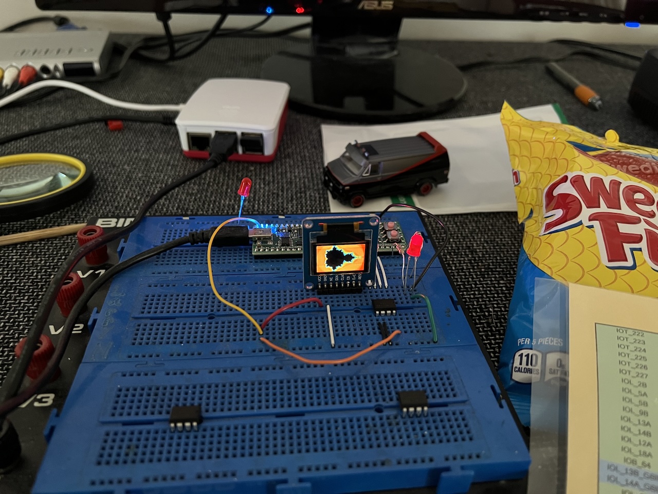
Here's the iceFUN board showing a Mandelbrot. It's connected to a Raspberry PI 5 which because all the FPGA tools are opensource can also be used for building the project.
Source code
https://github.com/mikeakohn/riscv_fpga
Copyright 1997-2026 - Michael Kohn
