x86 and 68000
FPGA
March 25, 2024
Introduction
Back in the 1980's, it seems the two most popular CPUs were the Intel x86 series and the Motorola 68000. The 68000 was used in the Amiga, Atari ST, Mac, Unix workstations, game consoles, arcade game systems, and even some guitar processors supposedly used it. The x86 series (8086, 80286, 80386, etc) was used in PC's and even today most computers sold at the stores are still using an updated 64 bit version of this architecture.
Everyone I know (including myself) that did 68000 assembly programming first and then got exposed to x86 was horrified by the x86 architecture. The 68000 had 8 data and 8 addressing registers (all 32 bit), a bunch of addressing modes, 32 bit ALU instructions, big endian, etc. The x86 was little endian, had segmentation registers (not anymore, but at the time this limited memory access to 64k), 8 registers that were semi-specific in functionality, and was originally only 16 bit.
In the past few years I ended up adding 68000 to naken_asm and my view of the chip actually kind of soured a bit. At my job I did some coding on a partial x86-64 assembler / disassembler and the instruction encoding didn't seem that bad. I've also got used to little endian and have seen some advantages of it as a programmer. Anyway, working on those two projects made me want to implement x86 and 68k in an FPGA and do a comparison of the two architectures.
This implementation has only the basic instructions of both chips. All addressing modes are supported, but many instructions that either aren't used much (or at all) or can be done with other instructions have been stripped out. An example would be anything BCD related or doing shifts / rolls directly on memory in the 68000. Both cores are 32 bit. The README.md file in the git repos for each gives a good idea of the list of supported / unsupported instructions, some that aren't listed may work and I may have left out some unsupported instructions too, but the important ones are listed I believe.
In a way I look at these implementations as... if x86 or 68000 could be put in a microcontroller, a complete instruction set that can do everything an avr8 or msp430 can do, this could be it. Each CPU has 8k of RAM and 4k of ROM, along with SPI, I/O, and some sound support. The FPGA used here is a Lattice iCE40-HX8K, not a very big chip.
Just like the previous CPU cores I did, neither of these do pipelining. I'm still learning this stuff, so maybe in the future.
All sample programs for x86 are assembled with nasm and all sample programs for 68000 are assembled with naken_asm.
Source code
https://github.com/mikeakohn/micro86
https://github.com/mikeakohn/micro68k
Related Projects @mikekohn.net
| FPGA: | FPGA VGA, Nexys2, Glow In The Dark Memory, Intel 8008, F100-L, RISC-V, x86 / 68000, MIPS, MSP430, PowerPC, W65C832, Apollo 11, PDP-11 |
Video
The video above shows each FPGA playing a song and then generating Mandelbrots side by side. On both FPGA's, the far right two columns show the program counter and the current CPU state. The first two columns on the 68000 show the bottom 16 bits of the d0 register and the x86 show the bottom 16 bits of the eax register (or just ax).
There is Java Grinder support for both 68000 and x86, so it could have been possible to do the music part of the demo in Java, but I would have had to check to make sure none of the unimplemented instructions were used. Plus, being in assembly, I like that when it pauses the code it doesn't trash d0 / eax so on the 4x8 grid of LEDs it's possible to see the binary representation of which note is currently being played.
Mandelbrots
The main test program for both CPUs is lcd.asm (lcd.asm for 68k and lcd.asm for x86). The code blinks and LED and when the user button is pushed generates a Mandelbrot on a 96x64 pixel OLED display sold by Parallax (SKU 28087). To code it up, lcd.asm from the RISC-V repo was cut and pasted part by part into the x86 and 68000 source files while translating the code to x86 and 68k assembly. Doing both at the same time was kind of awkward because of the reversal of src, dest in the assembler syntax. Because of the large register set, all variables were kept in registers in RISC-V, while both x86 and 68k keep all the variables in RAM. Also, serveral RISC-V instructions were sometimes able to fit in single x86 or 68k instructions.
As of this writing (it's possible there could be code changes), here are some stats:
| arch | size (bytes) | speed | LUTs | |
| x86 | 801 | 36s | 4077 | |
| 68k | 800 | 26s | 5454 | |
| RISC-V | 1116 | 23s | 7322 |
The RISC-V version was run on the RISC-V FPGA project completed a couple months earlier. Despite RISC-V having worse code density and needing more instructions to do the same tasks, it runs faster. Could be due to the 32 bit memory access and all local variables fit inside of registers.
Looking at the "speed" really doesn't tell the whole story. These implementations are not pipelined and the x86 has an 8 bit memory bandwidth that would slow it down. There is stuff that could be optimized too, for example in the x86 using "mov eax, 0" could be done as "xor eax, eax". The idea was to keep the assembly as human readable as possible.
Testing
Before getting into the deep details, just in case anyone is thinking of using this for something... this project really needs some kind of test that runs all possible combination of instructions and goes into a halt or error state if the result fails. Part of it was written for 68000 with test/self_test.asm in the repo, but it's very incomplete. That said, a lot of the instruction sets were exercised with the Mandelbrot code, but still there could still be bugs.
Starting Out
The x86, despite being a 32 (or 64 bit) CPU, has an 8 bit instruction set. Each opcode starts out as 1 byte and if more opcode is needed, more bytes are loaded. In some ways it almost looks like data compression with huffman encoding so it seems like code density should be tighter. More on that later.
The simplest instructions such as NOP and CWDE (sign extend ax to eax) are just 1 byte. Typically though, most instructions will require an extra byte or two along with possible immediate (or address) data. For this reason the x86 part of this project was started by copying the code from the Intel 8008 FPGA project and removing the 8008 code, replacing it with x86. The reason was the 8008 project used an 8 bit memory interface. I did consider the idea of optimizing with a 32 bit memory interface and some kind of 64 bit instruction cache thing, but the 8 bit model was a lot simpler.
The 68000 is also a 32 bit CPU instruction set, but every opcode is exactly 16 bits in size. There are cases when 1 to 3 more 16 bit words need to be loaded for immediate data and such, but everything is always in 16 bit reads. For this reason, this project started out as a copy of the RISC-V FPGA project with the memory interface narrowed to 16 bit.
Opcode Comparison
To start out with, here's 4 different uses of the "add" instruction in x86. The first 3 will add to the D register as 32, 16, or 8 bit (edx, dx, dl) from data stored at the address that the 32 bit esi register points to:
Assembly code:

// add edx, [esi]:      0x03,0x16
// add dx,  [esi]: 0x66,0x03,0x16
// add dl,  [esi]:      0x02,0x16

As bits:

prefix            dw  MD REG R/M
    -      0000 0011  00 010 110
0110 0110  0000 0011  00 010 110
    -      0000 0010  00 010 110

Reversed direction:

// add [esi], edx: 0x01,0x16

prefix            dw  MD REG R/M
    -      0000 0001  00 010 110
The first thing to notice here is that the 32 and 16 bit versions of the instruction differ only by an extra prefix byte at the start of the opcode (0x66). When using a register as 16 bit, this prefix is added to let the CPU know to run this instruction in 16 bit mode. So code density will be worse in 16 bit mode because of this extra byte which will incur more hits to memory, and therefore also have more latency. For the 64 bit versions of x86, 32 bit is still the default for data and indexing registers are 64 bit, so a prefix is needed to tell the CPU to use the data register as 64 bit or an indexing register as 32 bit.
This version of the add instruction has the binary format 1000 10dw. So the first 6 bits will be 100010, the d will tell the direction (write to the register from the effective address or store the value of the register to the effective address) and w, which if set to 1 will mean 32 bit and 0 for 8 bit. In the second byte, the 2 MD bits are the MODE, in this case reg, [reg]. The next set of bits tell which registers to use, in this case 010 is the D register, and 110 is esi.
The 68000 has equivalent instructions, note though that the syntax of the assembly language for is src, dest which is reverse of the x86 dest, src syntax:
Assembly code:

// add.l (a3), d2   0xd493
// add.w (a3), d2   0xd453
// add.b (a3), d2   0xd413

As bits:

               | ea  |
      REG  OP  MOD REG
 1101 010 010  010 011
 1101 010 001  010 011
 1101 010 000  010 011

Reversed direction:

// add.l d2, (a3)   0xd593

               | ea  |
      REG  OP  MOD REG
 1101 010 110  010 011
The postfix of .b, .w, .l tell the CPU to execute instructions for 8, 16, or 32 bit (byte, word, or long word). The first 4 bits should let the CPU know this is an add instruction, or really a regular add. There are adda, addi, addq, and addx (addx isn't supported right now in this core) that have different encodings. The next 3 bits are the source or destination register depending on the direction encoded in opmode (OP). A 1 says Dn + <ea> -> <ea> and a 0 says <ea> + Dn -> Dn. The bottom 2 bits of opmode tell the size of the data (00=byte, 01=word, and 10=long). The last 6 bits are the effective address (Dn, An, (An), (An)+, -(An), (d16, An), (d8, An, Xn * scale), (address).w, (address).l, #immediate, (d16, PC), and (d8, PC, Xn * scale). In these examples, an EA mode of 010 is (An) and the register is 3 so the effective address is (a3) which means grab data from the address that the address register a3 points to.
So far, other than 16 bit mode for x86, the code density of the two CPUs are even.
Some other interesting addressing modes, starting with x86:
// add edx, 3:             0x83,0xc2,0x03
// add edx, 10:            0x83,0xc2,0x0a
// add edx, 320:           0x81,0xc2,0x40,0x01,0x00,0x00
// add edx, [esi+32]:      0x03,0x56,0x20
// add edx, [esi+ebx*4]:   0x03,0x14,0x9e
// add edx, [esi+ebx*4+5]: 0x03,0x54,0x9e,0x05

[esi+32]    : address where to read data is esi + 32
[esi+ebx*4] : address where to read data is esi + (ebx * 4)
The same instructions with 68000:
// addq.l #3, d2            0x5682
// addi.l #0x0000000a, d2   0x0682 0x0000 0x000a
// addi.b #0x0a, d2         0x0602 0x000a
// addi.w #0x000a, d2       0x0642 0x000a
// addi.l #0x00000140, d2   0x0682 0x0000 0x0140
// add.l (32,a3), d2        0xd4ab 0x0020
// add.l (0,a3,d4.l*2), d2  0xd4b3 0x4a00

(32,a3)       : address where to read data is a3 + 32
(0,a3,d4.l*2) : address where to read data is a3 + (d4 * 2) + 0
Note that the scaling addressing mode (0,a3,d4.l*2) wasn't supported in 68000 until the 68020, but is supported in micro68k and was used while generating Mandelbrots to convert a count into a pixel color.
The 68000 has addq / subq instructions which can add or subtract a value between 1 and 8, and fits in a single 16 bit opcode. Otherwise, because the instruction has a .l postfix, the instruction will take 6 bytes. The x86, with an immediate between -128 to 127, will only take 3 bytes. If the 68000 instruction was .b or .w in size, it would take 2 words to describe the opcode (4 bytes). All opcodes are 16 bit aligned so even if data is only 8 bit, 2 immediate bytes are used and the first byte is wasted.
x86 also optimizes ALU things for the "A" register:
test eax,0x8000   a9 00 80 00 00
test esp,0x8000   f7 c4 00 80 00 00
This kind of seems like an idea that came from the old 8008 to 8080 CPUs. Originally the eax register was for math, edx is a data register, ecx is a counter register and had special instructions like loop and rep that auto-decremented it while doing other stuff, and ebx was for pointing at data. The esi and edi were.. seems like they were made to point at strings or such. So something like "rep movs" can be a single instruction to do a memcpy() using edi, esi, and ecx. I was tempted to implement movs and loop.. loop would be easy but I think it's deprecated in modern x86... movs wouldn't be too bad I think, but i was trying to keep size of the core down.
With both CPUs, if the CPU has 32 bits of data loaded in a register and a 16 bit or 8 bit instruction is executed on that register, the upper bits are left unchanged. So if the register has 0x12345678 and an 8 bit move of the immediate 0xff is operated on that register, the register will have the value 0x123456ff. The exception is an x86 CPU in 64 bit mode, a 32 bit operation does clear the upper 32 bits of the 64 bit register. Also the 68000 movea instruction with 16 bits to an address register will sign extend the upper 16 bits. The x86 separates the bottom 16 bits of each register into two 8 bit registers. So the bottom 16 bits of eax can be modified individually as ah and al.
The addressing mode that has a scaled offset is pretty interesting. These addressing modes are allow indexing into arrays of different sizes. In x86, if the MOD bits are set to 00 and the lower 3 register bits are 100, an extra byte called the SIB byte is loaded which contains 2 bits for the index size (1, 2, 4, 8), an index register, and a base register.
The 68000 version of the scaled offset which has an extra 8 bit constant for the offset is useful for indexing into an array or even an array of structures. x86 has the same thing, but the extra offset can be an extra 8 bits (1 byte) or 32 bits (4 bytes extra on the opcode).
C code:

uint32_t a[32];
uint16_t b[32];
int d = 4;

a[d] = c;
b[d] = c;

x86:

// mov [eax+edx*4], ecx
// mov [eax+edx*2], ecx

68000:

// add.l d2, (0,a3,d4*4)
// add.l d2, (0,a3,d4*2)
Speaking of code density, other more modern CPU's like RISC-V and ARM64 are pretty interesting. RISC-V (being a typical RISC CPU) has very small, simple instructions. In order to index into an array of 32 bit int's, the it takes 2 extra instructions to calculate the effective address (ea). Every instruction is also 32 bits so this ends up being:
RISC-V:

uint32_t a[32];
int d = 4;
a[d] = c;

// a0 is address to uint32_t a[32]
// t1 is index into the array
// t0 is data to store

slli t1, t1, 2   0x00231313
add a0, a0, t1   0x00650533
st t0, 0(a0)     0x00053283
The same thing can be done with ARM64 like this:
ARM64:

uint32_t a[32];
int d = 4;
a[d] = c;

// x4 is address to uint32_t a[32]
// x5 is index into the array
// w0 is a 32 bit register with data to store

str w0, [x4, x5, lsl #2]    0xb8657880
Despite the fact that the R in ARM is supposed to mean RISC, this architecture has some fairly non-RISC looking instructions / addressing modes. I have some mixed feelings about ARM64, but maybe having a fixed 32 bit opcode CPU with the same power of the instructions of x86 could be the key to being able to beat x86 performance? From implementing a lot of ARM64 into naken_asm, I found the bit encoding to be kind of upsetting.
Even though micro86 doesn't do 64 bit, it seems it might be interesting to show the code density on some 64 bit x86 instructions:
// add eax, [rsi]:           0x03,0x06
// add r9w, [rsi]: 0x66,0x44,0x03,0x0e
// add rbx, [rsi]:      0x48,0x03,0x1e
// add r9,  [rsi]:      0x4c,0x03,0x0e

// add eax, [rsi+32]:        0x03,0x46,0x20
// add rax, [rsi+32]:   0x48,0x03,0x46,0x20
// add eax, [esi+32]:   0x67,0x03,0x46,0x20 <-- danger!
// add r9,  [rsi+32]:   0x4c,0x03,0x4e,0x20
The first instruction with the default size 32 bit data, 64 bit addressing shows some great code density. Using a 64 register requires a single prefix, even if it's one of the new r8 to r15 regsiters that were added to AMD64. Using one of the r8 to r15 registers in 32 bit mode requires 2 prefixes. The addressing mode of using an indexing register plus an offset is interesting too when using a 32 bit register as an index. That requires a special prefix. In my experience, using the 32 bit esi accidentally instead of the 64 bit version rsi crashes the program every single time.
Memory Bus
As mentioned above, the micro86 connects to memory with an 8 bit data bus and the micro68k is 16 bit. So with the x86 core, an instruction with 2 bytes of opcode and 4 bytes of immediate data will have to go through 6 memory fetches to just load the instruction. With the 68000, an instruction with 1 word of opcode and 2 words of data will only have 3 memory fetches.
It seems like for most things, the 68000 will be faster just for the memory fetch model.
FPGA
Both cores are currently around 1600+ lines of Verilog. The FPGA used is again an IceFUN with a Lattice iCE40-HX8K with 7680 LUTs. I wanted to try the x86 on another FPGA board that has a Lattice LCMO2-4000HC with 4320 LUTs. Using the Icestorm tools (yosys / nextpnr) it seemed like it should fit, but nextpnr didn't support this chip. I ended up importing the source code into the Lattice Diamond tools, but it required more than double the LUTs that yosys / nextpnr needed for the iCE40-HX8K. I'm not sure if this is because the nextpnr does a better job with chip resources, or if the architecture is just so different that it requires more LUTs on that chip.
One thing that was nice about the Lattice Diamond IDE was it actually caught a bug and spit out an error. At some point in the x86 code there was [0:7] where it was supposed to be [7:0]. There were a couple other things that yosys allowed that Lattice Diamond didn't (using parameters before they were defined and leaving out begin / end in the tasks), but those didn't cause bugs.
The Verilog code itself is just a typical state machine. Fetch instruction, decode to figure out if it needs to grab effective address information, fetch effective address data, ALU computation, writeback to register or memory, etc. Other than the cluster-mess of trying to follow which state comes next when computing EA, the code should be pretty straight forward.
Features
Both the micro86 and micro68k have 4 banks of memory:
- Bank 0: RAM (4096 bytes)
- Bank 1: ROM (4096 bytes loaded from rom.txt)
- Bank 2: Peripherals
- Bank 3: RAM (4096 bytes)
Peripherals include SPI, IO, and MIDI note player. The README.md file in the repos explain more.
Differences
To keep the complexity down, it seems like the best thing to do would be to remove instructions that would never be used anyway and some that are very minor conveniences. An example of some instructions in x86 that are pretty pointless: aaa (ASCII adjust after addition), daa (decimal adjust al after addition), etc. Some instructions that are minor conveniences are loop (dec ecx and branch if not 0), push literal, etc.
All the ALU instructions, along with their strange addressing modes, should be available:
    mov eax, [ebx+0x4000]
    mov ebx, 0xf1
    mov [0x0004], ebx
    mov eax, [0x0004]
    lea eax, [ebx+eax*2]
    call eax
    test ebx, 1
    jz skip_led
    call led_on
    push ebx
    rol eax, cl
    shr eax, 5
The changes to 68000 are pretty much the same. All the addressing modes are supported, but unneeded instructions have been stripped out:
  add #0x1234, d0
  add d1, (0x0004).w
  add d1, (0x0004).l
  add d1, (a0)
  add d1, (a0)+
  add d1, -(a0)
  add d1, (1024,a0).l
  add d1, (8,a0,d1*4).l
  add d1, (1024,pc).l
  add d1, (8,pc,d1*4).l
All 8 registers in 8, 16, and 32 bit mode are supported with most instructions. The push / pop instructions only support a 32 bit registers.
In the 68000, the trap instruction is used to HALT the CPU. A trap #1 will put the CPU in the ERROR state and any other value will put the CPU into the HALTED state.
Odd Stuff
Both of these CPUs had some... opcode encoding decisions which kind of left me stumped.
The first is, the 68000's branch insructions. Most CPUs will compute the new branch offset by adding the offset from where the PC is after reading the full instruction. 68000 computes the new offset based on the PC after it read in the starting 16 bit opcode. Example:
0x4030: 6600 bne.w 0x4030 (-4)
        fffc
If the branch is taken, the new PC value is calculated by 0x4032 - 4 instead of 04034 - 4 like most CPUs would do. Oddly, some CPUs like RISC-V will caculate it based on the address of the opcode (in this case 0x4030) which kind of makes more sense than 68000, but still feels odd. This means there needs to be an extra FPGA register to keep track of what the offset should be added to.
I was also tripped up by the 68000 move.x instruction, which is encoded as:
.org 0x4000
  move.w (8,a4), (7,a5)

0x4000: 3b6c move.w (8,a4), (7,a5)
        0008
        0007

encoding of 3b6c:

         | d ea|  | s ea|
  00 SZ  REG MOD  MOD REG
  00 11  101 101  101 100
All instructions that have an "effective address" as a part of the instruction has it encoded in the bottom 6 bits (3 bits mode, 3 bits reg) of the instruction. Since "move.x" has 2 effective addresses, the destination effective address is the next low 6 bits (3 bits mode, 3 bits reg). Unfortunately, the designers of the chip flipped the 3 bits for REG MOD and I didn't realize this for a sad amount of time. I guess the reasoning was to help with opcode space for opcodes where bits 8:6 are an invalid mod.
Also, the bit encoding for the move instruction feels... wasteful in my opinion. Out of the 16 bits, the instruction has two 6 bit effective addresses encoded in it. In the example above, it lets the programmer have the ability to read in from memory and write directly back out without using a data register. It seems like it wouldn't be that big of a deal to break that up into 2 separate instructions burning a data register as a temporary. It would eat an extra 2 bytes to break it up, but it seems like it would make it easier to add extra instructions or 64 bit support or something. It also seems like doing complex data moves like that is very uncommon anyway.
Now for x86, some of the things that bothered me. The mod_rm byte that follows the opocde tells what the source / destination is. But Intel for complex addressing modes, the r/m register might be used to tell the CPU to load an extra SIB byte:
mov [ebp+edx+0],dx

66 89 54 15 00

  16 bit     mov      md reg r/m   S   I   B
0110 0110  1000 1001  01 010 100  00 010 101  0000 0000
                         edx esp     edx ebp      0
Depending on the mode (the 2 bits under md), if r/m is esp or ebp, then it will tell the CPU to lead an immediate or to load an SIB (scale / index / base) byte. In the example above, the the base register is ebp and the index is the edx register. This means doing what should be simpler addressing modes with esp or ebp requires the SIB:
mov [eax], edx: 0x89,0x10
mov [ebp], edx: 0x89,0x55,0x00
mov [esp], edx: 0x89,0x14,0x24

mov [ecx+4], edx: 0x89,0x51,0x04
mov [ebp+4], edx: 0x89,0x55,0x04
mov [esp+4], edx: 0x89,0x54,0x24,0x04
Those are some different instructions using a register as an index. Using [ebp] has to encoded as [ebp+0]. Using [esp] is worse. What's sad is ebp was typically used as a frame pointer for local variables of a function. Maybe it's not so bad since it would probably typically have +offset anyway.
Also, there's a bit in certain opcodes that I called "direction" that lets the CPU know if the result should go to or from a register / from or to memory. I had some issues with it. It's possible I goofed something up, but I had to create a flag that reversed the meaning of it sometimes.
The test, neg, and not (maybe other) instructions all shared the opcode of 0xf7/0xf6 (bit 0 tells if it's 8 bit or 32 bit). The way to tell which instruction is actually being used is in the mod_rm byte that follows the opcode in the "reg" spot (bits [5:3]). Maybe it's not that big of a deal, but I had some trouble with it. I didn't end up implementing the "not" instruction.. probably would be easy, but xor 0xffff does the same thing.
Pictures
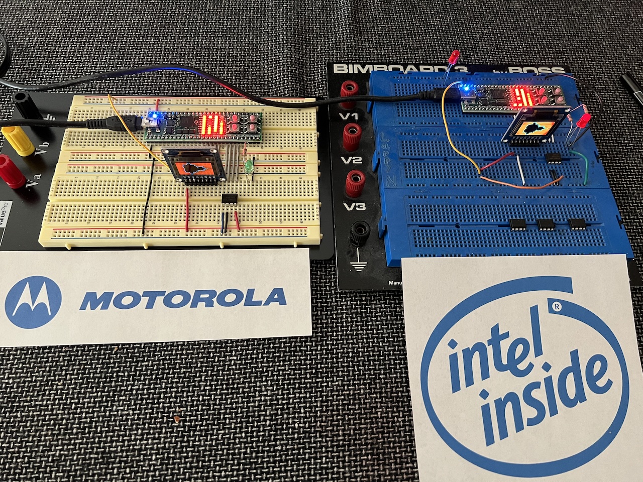
Here's a picture of the two boards after computing Mandelbrots.
Final Thoughts
The core of the micro86 was completed first and while working on the micro68k I kept thinking the x86 was actually easier. When it came time to run code and debug, I changed my mind and decided the micro86 is the more difficult of the two. They both have some pretty awkward things, but the x86 feels more like a compression scheme, having special versions of instructions for the A register, and mixing opcodes like neg and test in the same 1 byte of 0xf7, but the REG part of mod_rm will tell which instruction it actually is.. is just rough.
A part of me is now tempted to create a CPU instruction set that takes the best ideas of x86, 68k, ARM64, and RISC-V, but I think I'm going to take a break from FPGA for a little while.
Copyright 1997-2026 - Michael Kohn
