Cloud RAM
January 11, 2026
Introduction
With a new chip shortage beginning caused by big tech buying up RAM for servers for their datacenters, I came up with a solution for the problem. Introducing... Cloud RAM! Using the cloud, ordinary home computer users and businesses can rent and use the memory that big tech owns when their servers aren't busy computing AI slop videos for YouTube.
This project is a working proof of concept of the idea using an FPGA to implement it. The FPGA is wired to be a MIPS CPU that can do single word (4 byte) memory read / writes over a network cable to memory stored in a cluster of Raspberry Pi 4's. Essentially memory bus over UDP. The software running on this CPU has no idea this is happening.
Below is a full explanation how it works plus a video and link to the git repository.
Related Projects @mikekohn.net
| FPGA: | FPGA VGA, Nexys2, Glow In The Dark Memory, Intel 8008, F100-L, RISC-V, x86 / 68000, MIPS, MSP430, PowerPC, W65C832, Apollo 11, PDP-11 |
| Clusters: | Cloudtari, Mandelbrots, MSP430, Cloud RAM |
Video
YouTube: https://youtu.be/L25vYuHf160
The video is me trying to explain the system in under ~2 minutes. The first demo shows picture.asm running. All the executable code runs on local FPGA RAM, but the picture is stored at location 0xc000, so every pixel is a fetch to memory. The Verilog was written so that consecutive grabs to the same 4 byte area wouldn't cause another memory fetch, but I think that may be broken. Should be around 6,144 fetches. The second run (picture_main.asm and picture_draw.asm) puts the entire draw_picture function in the cloud so every instruction (minus the code in lcd_send_data) is a fetch to the cloud, along with every 16 bit pixel. When the image is done the server reports 37,126 memory fetches. Have to admit, I didn't expect it to run this fast. After getting it working and seeing the speed, I did kind of a "double take" trying to figure out if did something wrong.
Explanation
The components of this project are:
- iceFUN (Lattice iCE40-HX8K) FPGA board wired as a MIPS CPU.
- WIZnet W5500 (for networking).
- Four Raspberry Pi 4's running Kubernetes.
The CPU core is 32 bit and every instruction (every MIPS word) is 4 bytes. The memory_bus.v module therefore has a 32 bit data path to memory. There are 4 main memory banks accessable in the chip:
- 0x0000: Bank 0 - 4096 bytes of RAM
- 0x4000: Bank 1 - 4096 bytes of ROM
- 0x8000: Bank 2 - Peripherals
- 0xc000: Bank 3 - 16MB RAM
Accessing banks 0, 1, and 2 give immediate access to data / code since the memory is located inside the FPGA. Accessing any memory location 0xc000 or above will enable the circuitry in the cloud_ram.v module. That module will generate a UDP packet to send to a hard coded IP address requesting 4 bytes of memory. A return packet will either have the data or information of a new IP address / port to request memory from. The cloud_ram server has the ability to both load and store data.
Pictures
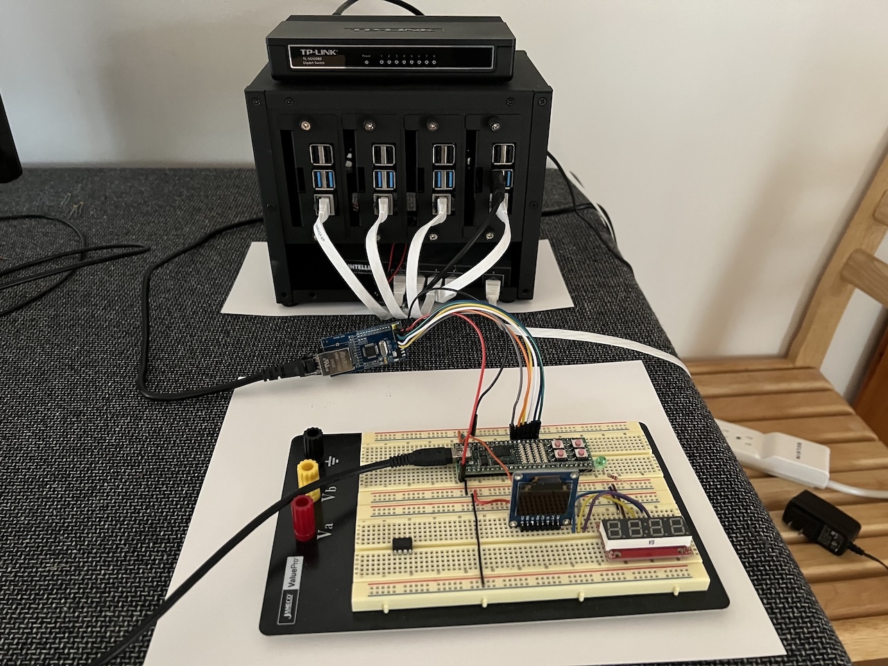
Above is a picture of the main setup. Towards the back is the "datacenter" which is four Raspberry Pi 4's and infront of it is a breadboard with the iceFUN FPGA. To the back of the breadboard is the WIZnet W5500 board connected to the FPGA.
MIPS CPU
Over the past few years I've put together a few FPGA CPU cores, so there were a few to choose from. I went with an implementation of MIPS since it's one of the simplest cores, almost the same really as RISC-V but I find the MIPS instruction set a little cleaner in some ways. The design here is pretty much 5 CPU cycles per instruction and not pipelined. Can probably be taken down to 4 cycles, but I'm still learning this stuff. The steps taken to execute instructions for the most part come down to these steps:
1: FETCH instruction start
2: FETCH instruction finish
3: DECODE
4: EXECUTE
5: WRITEBACK (either register or memory)
One of these days I'll combine steps 1 and 2, but for now, this is what's going on. So looking at the following instructions:
.org 0x4000
main:
  li $a1, 0xc000    (alias for: or $a1, $0, 0xc000)
  lb $t1, 0($a1)
The code above first sets the $a1 register to 0xc000 to be used as a pointer. The second instruction loads 1 byte from memory location $a1 + 0 (effective address being 0xc000) into the $t1 register and sign extends it to 32 bit. Since .org is set to 0x4000, the executable code is sitting in memory location 0x4000. So back to the steps taken to execute those two instructions:
1: FETCH  - 32 bits from memory location 0x4000
2: FETCH    Finish loading the instruction into the CPU.
3: DECODE
4: EXECUTE
5: WRITEBACK ($a1 now equals 0xc000)

1: FETCH  - 32 bits from memory location 0x4004
2: FETCH    Finish loading the instruction into the CPU.
3: DECODE
4: EXECUTE (request 32 bits from location 0xc000 ignoring bytes 1-3)
5: WRITEBACK ($t1 now holds the value from 0xc000).
During the fetch for location 0xc000, the cloud_ram.v circuit is activated. That piece of circuitry is a state machine with 15 states that will tell the WIZnet W5500 chip to send out a UDP packet to a specified IP address requesting a memory load or store. The chip will wait for the server to respond with a UDP packet that has the data loaded, or a UDP packet confirming the store was successful, or a UDP packet that redirects the CPU to a different IP address / port. If a redirect happens or a timeout waiting for the UDP packet happens, the CPU will repeat the request.
Whenever the cloud_ram.v circuitry is activated, a mem_bus_halted signal is set high. When the signal is high, the MIPS CPU goes into a wait state until the memory request is ready.
The Cluster
The main program running on the cluster is cloud_ram.c. To make debugging easier, the data is not actually stored in RAM, but is stored in a file. Would be quite simple to make it either pure RAM or maybe better mmap()'d, but debugging was important. The cloud_ram program has the ability on startup to read in a file called preload.bin into the memory region. This gives the ability to put data or even executable code into memory.
The protocol consists of UDP packets with this structure:
struct Packet
{
  uint32_t address;
  uint16_t length;
  uint8_t write_mask;
  bool save_data  : 1;
  bool read_only  : 1;
  bool is_address : 1;
  uint8_t data[8];
};
Address is the memory location to start the read / write from while length is how many bytes to transfer. In this example the length is always 4. The save_data bit tells the server that the operation should be a store to RAM using 4 bits of the write_mask option to tell the server which of the 4 bytes in the 32 bit word really need to be written. The read_only bit lets the CPU know that the area being access is read only. In this example memory locations 0xc000 to 0xffff are hardcoded as read only. The is_address flag tells the CPU that the information in data is a new IP address / port to connect to (maybe a confusing name).
Whether the instruction is a read or write, the server will return a packet back to the CPU. The CPU has a timeout period where if it doesn't get this response it will request the load / store again.
The cloud_ram executable is run from a hardcoded IP address so the CPU always knows where to connect to. When running as a cluster, instead of running cloud_ram on the main IP address / port, a Python script called cloud_route.py is run instead. When cloud_route.py detects a UDP packet, it will tell Kubernetes to start a new pod that runs the cloud_ram executable and send a UDP packet back to the CPU telling it what the new IP address / port is.
The two hardest parts of this project ended up being Kubernetes and figuring out how to get the WIZnet W5500 working. I was tempted to leave some notes here about how to get Kubernetes setup incase it would help someone else or a future me working on a new project, but... Kubernetes. Yeah, Kubernetes. So speaking of WIZnet W5500...
WIZnet W5500
For the networking support, a small board with a WIZnet W5500 chip was used. The chip communicates with the FPGA over an SPI bus. The chip is capable of both TCP and UDP, and does all the "fun" parts of networking including ARP.
I ended up getting a pair of these from Amazon, but was having such a hard time getting them working so I got a couple from a different manufacturer just to make sure the boards weren't bad.
Before implementing this in an FPGA, it seemed better to get it working in an MSP430 first (w5500.asm) since it's a lot easier to debug. There's an order things had to be done otherwise things just didn't get initalized properly. Setting the destination IP address / port etc for example didn't seem to work until the PHY was ready. The order that I found got things working:
  Hold RST low for ... maybe 500ms.
  Hold RST high for the same amount of time.
  Read MODE_REGISTER (0x0000) until RST bit goes low.
  Read PHYCFGR (0x002e) until LNK goes high.
  Set in Common Register Block:
    - Gateway address.
    - Subnet mask.
    - Hardware address.
    - Source ip address.
    - Interrupt low level timer.
    - IR (to clear interrupts).
    - IMR (internet mask register).
    - SIR (socket interrupt).
    - SIMR (socket interrupt mask).
  Set in Socket Register Block:
    - IMR (Socket Interrupt Mask).
    - Sn_TXBUF_SIZE (4k).
  Open UDP Socket:
    - Set Sn_MR (Socket Mode) to UDP.
    - Set Source Port.
    - Set Destination Address.
    - Set Destination Port.
    - Set Cn_CR to OPEN.
    - Read Sn_SR. If it's not OPEN, repeat previous steps.
That should be the steps to initialize the network and open a UDP socket. It's possible that if the chip isn't connected to the network, that the PHY will not go to UP and destination IP addresses can't be set.
Setting up the WIZnet in an FPGA was quite interesting. For this project there is a file called commands/w5500.asm. The file is basically just a bunch of .db data bytes that gets assembled with naken_asm. Each .db byte block contains first the number of bytes to clock out of SPI and then a block of byte to be clocked out. If the length is 0xff, it means stop clocking out bytes. Before each block the SPI /CS is set low and when all the bytes for the block are clocked out the SPI /CS pin is set high. The .db blocks were supposed to be loaded into the FPGAs BRAM, but at some point some Verilog made it impossible for yosys to infer them as BRAM. The cloud_ram.v circuitry modifies some of that data at certain points.
As stated earlier, the cloud_ram.v module is a state machine of 15 states. The first few states are mostly for initializing the W5500. There are a few states that do the SPI. Those states are referenced from states that stream sequences of bytes from the w5500.asm file. It's some interesting code.
It does seem that one of the original WIZnet W5500 modules I got doesn't work. Same code that works on 3 of the boards doesn't work on the 4th.
Final Thoughts
I was kind of surprised how quick the memory was, but clearly this thing isn't practical. This project was really supposedly be more of functional tech satire rather than being anything useful.
That said, I did have the thought that maybe it could work a little bit more like cache or virtual memory. Have a couple small buffers of 128 bytes, or maybe even 4096 bytes and keep a table of mappings from the requested address to where that data exists in a local buffer (TLB). If the mapping doesn't exist, writeback local memory to the cloud and read from the cloud into local memory.
Doing something like this with Linux should also be possible using the virtual memory system. At minimum a swap file could be created and placed on something like an NFS server. It might also be possible to create a kernel module that uses the same Kubernetes system where pages that are swapped in / out could be UDP packets to the cloud.
This also could be used as more of a bootstrap-like system. Currently, in order to populate the rom.v portion of the FPGA, the code is copied to a rom.txt and built into the .bin file along with the Verilog code. This means changes to the software that runs on the MIPS core can take 1 to 5 minutes to build. But for now, this project is done.
Source Code
git clone https://codeberg.org/mikeakohn/cloud_ram.git
Copyright 1997-2026 - Michael Kohn
